info@biomedres.us
+1 (502) 904-2126
One Westbrook Corporate Center, Suite 300, Westchester, IL 60154, USA
Site Map
Received: April 26, 2024; Published: May 09, 2024
*Corresponding author: Slah Hlali, Laboratory of Microelectronics and Instrumentation (LR13ES12), Faculty of Sciences of Monastir, Avenue de l’environnement, University of Monastir, 5019 Monastir, Tunisia
DOI: 10.26717/BJSTR.2024.56.008869
This study investigates the electrical properties of the novel MIS structure TiN/Al2O3/P-Si through C-V and I-V analyses, employing Silvaco TCAD software for simulation. Examination of various parameters including frequency, temperature, oxide thickness, surface conditions, and doping levels reveals their impact on the device characteristics. The simulation results align well with theoretical expectations, validating the proficiency of the simulation approach. Temperature variation is found to influence the flat band voltage, possibly due to changes in oxide charge density and interface defect density, while a weak inversion zone is observed within a temperature range of 77 K to 300 K. Frequency dependence is notable, particularly at 1 GHz, affecting the C-V behavior significantly. I-V analysis uncovers asymmetrical temperature activation, indicating the presence of dual conduction mechanisms. Moreover, higher doping levels correlate with increased current density in the negative voltage regime. Simulated leakage currents for capacitors with varying dielectric thicknesses suggest non-uniform behavior, with electron injection from the gate leading to higher current density compared to the substrate due to band diagram asymmetry. This underscores the influence of decreasing oxide thickness on leakage current behavior.
Keywords: High-K; Metal/Insulator/Semiconductor (MIS); Numerical Simulation; C-V; I-V; Al2O3/Si Interface
An MIS capacitor, also called MOS in the case where the insulating layer is oxide-based, is a structure formed by the superposition of Metal - Insulator - Semiconductor heterojunctions. It is one of the most important elementary components in microelectronic technology, it provides the conduction channel for MISFET transistors (MOSFET), it is also an essential element for the characterization of epitaxial layers, or to evaluate the potential of a technology. This structure has been widely studied in recent decades. The study of the electrical characteristics of MIS devices is of great importance for understanding the physical characteristics, such as the nature of the interface between the semiconductor and the insulator. This structure can be compared to a capacitor made up of two conductive electrodes separated by an insulating material [1]. The MIS diode is the most useful device in the study of semiconductor surfaces. Indeed, the reliability and stability of all semiconductor devices are extremely linked to their surface conditions.
Following the increasing miniaturization of MOS devices, silicon oxide (SiO2) has reached these limits where it is necessary to use dielectrics other than SiO2 (𝜀𝑟 = 3.9) to be able to amplify the capacitance per unit of surface. The use of high permittivity dielectrics and a solution allowing a capacitance value equivalent to SiO2 with larger films. In this case, we can limit the leakage current through the gate oxide (insulator) and reduce the value of the electric field which is the cause of electrostatic breakdown as well as leaks in the structure. For gate contacts it is preferable to use metals whose output work is high so as to increase the height of the potential barrier at the interface which leads to the reduction of leakage current and thus avoid problems of poly-depletion. The introduction of new metallic materials and High-K materials (strong insulators Permittivity) becomes mandatory in future generations of MIS capabilities, in order to achieve the desired performance. These materials have very good intrinsic properties but certain problems appear from their integration into technological sectors.
The Objectives Pursued in this Work are Divided into Two Parts
The first will concern the study of capacitance as a function of voltage for different frequencies and for different surfaces. Subsequently, we will study the effect of the thickness of the oxide, the doping of the substrate as well as the effect of the temperature variation on the capacitance of our structure. The second objective of this report will focus on the study of current density as a function of voltage while varying certain parameters such as the effect of oxide thickness, doping and the temperature of the MIS structure. We used the TCAD “Computer-Aided Design Technology” to make a comparative study of the electrical behavior of the metal-insulator-Semiconductor Schottky diode with different parameters such as doping, thickness of the insulator, temperature, etc. TCAD contains physical models for the description and simulation of semiconductor devices. It completely imitates the technological processes of Semiconductor. Essentially it acts as a virtual fabrication. The structure of a device is approximated by a finite number of discrete elements called “MESH”, which can be one-dimensional, two-dimensional or three-dimensional.
Silvaco TCAD software is used to simulate the electrical characteristics of the two-dimensional MIS structure. This structure has a surface area of 100*100 um2 manufactured on P-doped silicon with a value of 1e16 cm-3, and then a thickness of 5 nm of Al2O3 is deposited just below a TiN metal grid.
The essential properties to consider for the gate oxide are:
1. The value of the permittivity
2. Band structure
3. The discontinuity of the bands for the transport of loads
4. Thermodynamic stability
5. The quality of the interface with the Si
6. The morphology of the film
7. Compatibility with the gate electrode and with the technological
process
8. Reliability [2,3].
The main “high-κ” materials and their properties are presented in Table 1. Al2O3 oxide is widely studied as a dielectric of capacitive structures, its thermal capacity is equal to 1.97 J/K.cm3 and its thermal conductivity is equal to 33W/K.cm3.
Table 1: Properties of high-κ materials (according to [4- 8]).

Figure 1

In this part we will study the variation of the capacitance as a function of the voltage of the MIS structure and have the effect of different variables (like temperature, doping and etc.) on the capacitance curve. The curve in Figure 2 represents the variation of the capacitance as a function of the voltage of the MIS structure: TiN / Al2O3 (5nm) / p-Si with a surface area of 100*100 um2 and at high frequency and for a p-doped silicon substrate of value 1e16 cm-3. The C-V curve is very close to reality, which validates the simulation results. The characteristic of the capacitance as a function of the gate voltage makes it possible to give the capacitance of the Cox oxide and to approximately determine the operating regimes of the structure: the accumulation regime, the depletion regime and the inversion regime. The accumulation and depletion regimes appear clearly, the inversion regime is generally more difficult to observe on silicon-based MIS structures at room temperature, due to the low generation rate of minority carriers, the deep depletion regime is more often reported in the literature [5,6]. The accumulation capacity is equal to 21nF. From the curve of (1/C2) - V presented in Figure 3, it is possible to determine the flat band voltage (VFB) which corresponds to the intersection of the tangent to the curve (1/C2) - V in depletion regime and the axis of tensions. The flat band voltage obtained from curve 3 is VFB = - 0.5V and the capacitance CFB ≈ 12 nThe shift of the flat band voltage (VFB = - 0.5V) is due to the difference in the output work Фms between the metal and the semiconductor, to the fixed and moving charges present in the insulating layer and to the charges of interface to the Al2O3/Si interface. VFB can be written in the form
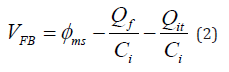
Where Qf fixed charges, Qit the interface charges and Ci the capacity of the insulating layer.
Figure 2

Figure 3

We notice by continuing the polarization, the majority carriers are increasingly pushed back from the insulator-semiconductor interface, the thickness of the ZCE is then maximum W=Wmax, such that
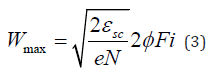
With ε_scthe dielectric permittivity of the semiconductor and Ф_ Fi given by the Eq. (4):
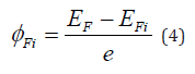
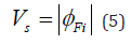
The curvature of the energy bands increases, and for a certain voltage, the intrinsic Fermi level E_Fi falls below the Fermi level E_ Fsc of the doped semiconductor. The surface potential Vs reaches a threshold for which the majority carrier density at the interface is equal to the minority carrier density in the semiconductor.
The threshold corresponding to the transition between the depletion regime and the inversion regime is defined by Eq. (5):
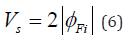
In the inversion regime, the charge at the interface is conditioned by the depletion charges because the minority carriers are in negligible quantity compared to the density of the dopants. On the contrary, in the strong inversion regime, the charge at the interface is conditioned by the minority carriers whose density, on the surface, is much greater than the density of the dopants. The threshold Vs, for which the density of minority carriers is equivalent to the density of the dopants (p=Nd for type N or n=Na for type P), is defined by Eq. (6):
The gate voltage corresponding to this condition is called threshold voltage VTH [7]:
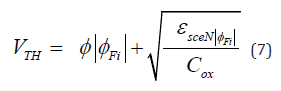
With Cox the surface capacity of the oxide expressed in F.m-2.
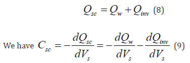
Figure 4 presents the energy band diagram, the charge distribution and the electric field distribution in an ideal MOS structure on a P-type substrate in the inversion regime [8]. The total charge in the substrate is the sum of the charges from the dopants of the QW semiconductor in the ZCE and the minority carriers accumulated at the Qinv semiconductor insulating interface. In inversion regime, the charge in the semiconductor is written by Eq. (8):
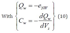
The capacity of the Csc interface is maximum in inversion mode, because the ZCE is maximum (W=Wmax). The total capacity of the structure is then written by Eq. (11):
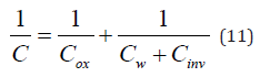
With Cox the capacitance of the oxide, Cw capacitance due to the ZCE and Cinv capacitance due to the minority carriers accumulated at the insulator-semiconductor interface as shown in Figure 5.
Figure 4

Figure 5

Study of the Capacity for Different Values of Oxide Thickness
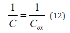
In this part, we vary the thickness of Al2O3 to show the influence of the thickness of the oxide on the C-V curve while retaining the doping at 1e 16 cm-3 and the frequency at 1KHz. Figure 6 gives the simulated C-V characteristics for different Al2O3 thicknesses over five 100*100 μm² MIS capacitors comprising TAl2O3 oxide thicknesses of 1, 2, 3.4 and 5 nm. From this curve we notice that the variation in the thickness of the oxide acts on the C-V characteristic at the level of accumulation and depletion regime, while at the inversion regime no variation is observed. Indeed, for semiconductors whose majority carriers are holes (P-type semiconductor), an accumulation of majority carriers is formed at the insulator-semiconductor interface for Vg&less;VFB. In a first approximation, the capacity of the interface can be negligible and the equivalent capacity of the structure is then written by Eq. (12):
Indeed, in accumulation, the MIS capacitance is equivalent to a plane capacitor with a thickness equal to the thickness of the Tox insulation and whose capacitance of the insulating layer is given by Eq. (13):
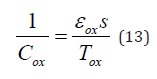
Figure 6

From this last equation and Figure 6, we can see that the difference between the C-V curves increases with decreasing oxide thickness. Indeed, the more the thickness of the oxide decreases, the greater the quantum confinement effects, thus leading to a strong overestimation of the capacity (Figure 7). The work output of the TiN electrode will be determined from the value of the flat band voltage using the relationship Eq. (14):
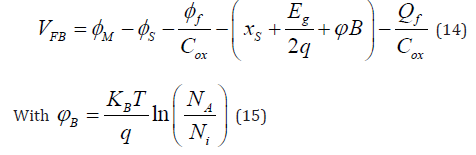
Figure 7

Figure 8

Determining the output work of the electrode requires a priori knowing, in addition to the flat band voltage, the density of fixed charges in the insulator Qf. However, it is possible to overcome this parameter by defining the flat band voltage that we would have in the absence of oxide. This is obtained by extrapolating the VFB-tox characteristic presented in Figure 8 for a zero Al2O3 thickness. The flat band voltage obtained in this case is equal to -0.64 V. This value then corresponds to the difference between the output work of the electrode and the semiconductor 𝜙M - 𝜙S. Depending on the characteristics of the silicon substrate (NA= 1e16 cm-3 and Ni= 1010 cm-3 gives 𝜙S = 5eV) we obtain for the TiN electrode deposited on Al2O3 an output work equal to 4.36 eV. Extrapolation of the curve for zero Al2O3 thickness makes it possible to overcome fixed charges in the oxide.
Study of the C-V Characteristic for Different Surfaces of the MIS Structure
The surface of the structure having great importance in the field of nanoelectronics, for this the study of the capacitance as a function of the voltage for different surfaces is given in Figure 9. This figure shows the proportionality relationship between the capacitance and its surface as shown by the Eq. (16):
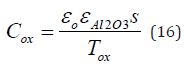
Figure 9

We notice from this curve that the value of the capacity in the accumulation regime increases with the increase in the surface area of the structure. In the inversion regime we notice that there is superposition of the capacity curves for different surface values. We therefore deduce that the surface of the MIS structure acts on the C-V characteristic only at the level of the accumulation and depletion regime.
Study of the C-V Characteristic for Different Doping Values of the Substrate
In this part, we present a modeling to simulate the effect of substrate doping on the C-V characteristic of our TiN / Al2O3 (5nm) / p-Si structure for a surface of 100*100um2 and at high frequency 1KHz. The deformations of the C-V curves generated by various doping values are presented in Figure 10. The uniformity of the insulation thickness over the entire surface of a wafer (silicon wafer) is a key parameter to guarantee the same characteristics electrical connections from one component to another. This curve shows the evolution of the C-V curve as a function of the doping of the substrate. The parts of the C-V curve that depend only on substrate doping correspond to the substrate depletion and inversion regime. On the other hand, the accumulation regime is not affected by this variation in the doping profile. The voltage of flat bands varies with the variation of the doping value on the C-V characteristic of the MIS structure. The Nsub doping concentration of the substrate is related to the inverse of the slope of the 1/C2 curve as a function of the VG voltage. The doping concentration is calculated by [9] (Eq. (17)):
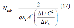
Figure 10

Study of Capacity as a Function of Frequency
In this part we studied the variation of the capacitance as a function of frequency for our MIS structure with a surface area of 100*100 um2 and for a doping value equal to 1e16 cm-3. Figure 11 shows the simulated C-V characteristics for varying ac signal frequencies from 1 kHz to 1 GHz. The high frequency C-V characteristics show a strong decrease in capacitance for frequencies above 1 MHz, this demonstrates the presence of a high density of states in the oxide, and these states can follow the low frequency ac signal, but cannot follow the AC signal for high measurement frequencies, which causes the capacitance (dispersion) to drop. Dispersion can also result from series resistance created by the lightly doped semiconductor [10]. We deduce from this curve that the effect of frequency on the C-V characteristic only appears for the 1 GHz frequency whereas for the 1 KHz, 10 KHz, 100 KHz and 1 MHz frequencies the C-V characteristics do not change and are superimposed on each other, on the other. The capacity decreases for the 1 GHz frequency and reaches a value of around 1.4e-10 F. We also note that the variation in frequency only acts on the accumulation regime of the C-V curve.
Study of Capacity as a Function of Temperature
Figure 12 represents the variation of the capacitance as a function of the voltage for different temperature values ranging from 77 K to 800 K and for a frequency of 1 KHz. The variation of the temperature for the MIS TiN / Al2O3 (5nm) / p-Si structure leads to the variation of the C-V characteristic for the three operating regimes (accumulation, depletion and inversion). We also note that the increase in temperature is accompanied by the decrease in the flat band voltage, and this may be due to the reduction of the total charge density in the oxide and the defect density at the interface [11]. At low temperature 77 K up to ambient temperature 300 K, the C-V characteristic has a weak inversion zone while beyond 300 K we find a strong inversion zone; here the holes are pushed back with the appearance of an electron- rich layer near the semiconductor interface.
Figure 11

Figure 12

Grid Current
The search for a minimum gate current density is a determining element in the integration process of high-K oxides. In Table 2 we find some examples of current density reported on Al2O3 by different authors. Compared to SiO2, the Al2O3 oxide leads to a reduced current density of the order of 2 to 3 decades [12].
Table 2: Current density reported for Al2O3 oxide by several authors.

Current-Voltage Characteristics
Figure 13 shows the variation of the absolute log of the current density as a function of the voltage Vg applied to the MIS structure at ambient temperature. From this graph, we see that:
a. Current density increases for voltages above and below 0.3V
b. The current characteristic in the case of SiO2 is the same as
that of Al2O3, which shows that the injection mechanism is the same
for both structures.
c. At the same oxide thickness of 5nm, we notice that the current
density of the High-K oxide Al2O3 is greater than that of the standard
oxide SiO2 (shift of two decades).
d. The rapid increase in current density observed in the case
of the metal grid structure suggests a Fowler-Nordheim type conduction
mechanism. The current-voltage characteristic was modeled by a
Fowler-Nordheim model in the accumulation regime (forward polarization
regime) and inversion (reverse polarization regime) of silicon.
e. The shift from zero in the current density is explained mathematically
by the following equation Eq. (18):
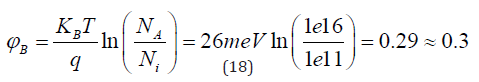
Figure 13

Current Versus Voltage for Different Thickness of Al2O3 Oxide
In this paragraph we will see the effect of the Al2O3 oxide thickness on the current behavior of the MIS TiN/ Al2O3 / P-Si structure with a surface area of 100x100 μm². In Figure 14 we represent the simulated leakage currents in negative polarization (injection of electrons through the upper interface) and in positive polarization (injection of holes through the lower interface) in seven TiN/ Al2O3 / P-Si capacitors, whose dielectric thickness varies from 4 to 10 nm each time. In this case, the curves overlap with a shift of approximately 3 decades by a variation of 1nm in the thickness of Al2O3 oxide. It can be noted that the current density is higher for injection from the gate than from the substrate. This phenomenon is due to the asymmetry of the band diagram of the structure [13-18]. The position of the charge does not have the same impact on the two currents because the probability of passage of electrons is different depending on the injecting electrode (grid or substrate). The asymmetry, observed when the current decreases, suggests a non-uniform distribution of charges trapped in the insulation. In this case the leakage current through the oxide increases with decreasing oxide thickness.
Figure 14

Current Versus Voltage for Different Substrate Doping Values
For the same surface S = 100*100 um2, the TiN/ Al2O3 / P-Si structure was simulated for different doping values ranging from an undoped substrate to a doped substrate 1e16 cm-3 as shown in Figure 15. We note that the current density is minimal in the negative voltage regime for the undoped MIS structure, whereas in the positive voltage regime the current density does not depend on the substrate doping values. In the negative voltage regime the current density increases with increasing doping values.
Current Versus Voltage for Different Temperature Values
The temperature dependence with leakage current is studied to understand the current transport mechanism. This current is simulated in a temperature range of 280K up to 440K with a step of 20K as shown in Figure 16.
Figure 15

Figure 16

Depending on the direction of injection of the carriers, we can observe a significant asymmetry in terms of temperature activation.
1. Injection of electrons from the grid (VG < 0): In the MIS structure,
very weak temperature dependence is observed and this
confirms that the predominant conduction mechanism is of
the Fowler Nordheim type.
2. Injection of electrons from the substrate (VG > 0): In the regime
of injection of carriers from the substrate, the temperature
dependence is greater, which indicates that the conduction
is assisted by traps (notably in the Al2O3 dielectric of 5
nm), unlike Fowler Nordheim type conduction.
The research focuses on exploring the electrical characteristics C-V and I-V of the MIS structure TiN/Al2O3/P-Si, simulated using Silvaco TCAD software. The analysis showcases proficiency in simulation techniques, with numerical simulations aligning well with theoretical curves from literature. Notably, asymmetry in temperature activation based on carrier injection direction is observed, with weak temperature dependence in electron injection from the grid indicating Fowler Nordheim conduction and greater temperature dependence in electron injection from the substrate suggesting trap-assisted conduction. Moreover, increasing doping values lead to higher current density in the negative voltage regime. The study also highlights that the surface and oxide thickness of the MIS structure significantly influence the C-V characteristic during accumulation and depletion regimes. Additionally, the temperature-dependent analysis of the MIS TiN/ Al2O3/P-Si structure reveals variations in the C-V characteristic across accumulation, depletion, and inversion regimes. As temperature increases, there is a decrease in flat band voltage possibly due to reduced total charge density in the oxide and interface defect density. Notably, a weak inversion zone is observed at temperatures between 77 K and 300 K, transitioning to a strong inversion zone beyond 300 K where an electron-rich layer near the semiconductor interface repels holes. Frequency also plays a significant role in the C-V characteristic, particularly at 1 GHz, impacting the accumulation regime notably.
Dr. Slah Hlali would like to express his gratitude and thanks for his funding by the Tunisian Ministry of Higher Education and Scientific Research, which enabled him to carry out his research and provided him with all the necessary assistance.
The authors (Slah Hlali, Neila Hizem and Adel Kalboussi) declare that they have no conflict of interest.
Thanks to microelectronic and instrument laboratory (μEi)group.