info@biomedres.us
+1 (502) 904-2126
One Westbrook Corporate Center, Suite 300, Westchester, IL 60154, USA
Site Map
Received: May 15, 2023; Published: June 05, 2023
*Corresponding author: Florin Gaiseanu, Research Professor, Science and Technology of Information (Bucharest Romania) and (Barcelona Spain), Spain
DOI: 10.26717/BJSTR.2023.50.008015
In this paper are shortly presented advanced results on the design and fabrication of the silicon capacitive
sensors for biomedical applications, obtained by the Bulk Micromachining (BMM) technology, based on
an analytical modeling of the boron diffusion in silicon at high concentrations, suitable to describe both
the boron diffusion and etching process of silicon for thin membrane achievement. The boron diffusion
in silicon for the fabrication of the silicon capacitive sensors for biomedical applications and other
Microelectromechanical Systems (MEMS) is a critical process, because the boron diffusion profile depends
on the diffusion oxidizing (BBr3, B2O3)/non-oxidizing (BN – Boron Nitride) sources, and furthermore,
the subsequent etching rate (so the etching time), depends on the depth distribution x of the boron
concentration C in the silicon bulk, so an accurate simulation of this profile C(x) allows the accurate etching
process for membrane design and fabrication. For this, analytical explicit relations are presented for the
boron diffusion and etching process, applicable to the described cases (BBr3, B2O3 or BN using), and also a
general form of solutions of the non-linear diffusion equations with diffusion coefficient D depending on
the concentration C as D~Cm (m – a real number), explicitly expressing the diffusion profile in the silicon
bulk as C=C(x), and also as a reverse relation x=x(C), for easy calculation of this geometrical parameter for
a given value of C.
This set of relations can be used not only to design and fabricate pressure sensors or other MEMS
structures by BMM technology with well-defined geometrical characteristics, but also for the optimization
with respect to the diffusion gradient, which induces mechanical stress into membrane. With this respect,
the results show more reduced gradients after diffusion from BN sources near the silicon surface, than that
from oxidizing sources.
Keywords: Boron Diffusion; Design/Fabrication; Silicon Capacitive Sensors/MEMS Structures; Oxidizing (BBr3, B2O3)/Non-Oxidizing (BN) Sources; Vacancy/Interstitial Assisted Diffusion; Chemical Etching Rate and Etching Time, Analytical Results; Intrinsic Stress
The microelectronic circuits fabricated on silicon substrate material became nowadays imprescriptible components of the informational systems, either used in communication [1,2], for decisional [3] or medical applications [4,5], or in other artificial intelligent systems [6], because the silicon planar technology [7,8] allows the achievement of cheap production of high quantity chips in the same cycle of fabrication. The application of such technology for the preparation and fabrication of the silicon capacitive sensors, defined as microelectromechanical systems (MEMS) [9,10], in combination with the tridimensional (3D) Bulk Micro-Machining (BMM) processing by chemical etching methods, is therefore of high interest for their increasing development. That is because of their large range of applications, not only in the healthcare and biomedical field [11], due their bio-compatibility, micro-miniaturization and integrability for measurements in-situ or fitted to catheters, in respiratory and airflow circuits [12], or in operative microelectronic telemetric [13] and Lab-stations lines [14,15], but also in industry, automations and automobile domains, military/civil aviation and even in common consumer electronics fields [16].
In particular, the silicon capacitive pressure sensors for biomedical applications are used for the measurement of blood pressure under highly sensitive/small dimension conditions, like in the intraocular/intracranial zones for glaucoma/hypertension/ inflammatory dysfunctions/diseases, in microsurgery, diagnosis and micro-therapy processes [16]. The functioning of the silicon capacitive pressure sensors is based on the measurement of the variation of the capacity C =ε ( A / d ) between two electrodes of area A placed at a distance d, into a medium (in particular air) of permittivity ε , which rely on the displacement of a silicon membrane suspended above of a fix delimitated isolating support on the substrate electrode [17]. Under dynamic conditions, the value of displacement depends on the geometrical dimensions, i.e., on the area A, the distance d between the electrodes and on membrane thickness, so that the constructive designed/technological parameters are critical/decisive for the final performances of the pressure sensing device [17,18].
Taking into account the high importance of such requirements, the improved precision of the design and control of the technological processes for the fabrication of the silicon capacitive sensors for biomedical applications and other MEMS devices, is really necessary. Therefore, in this paper are presented some recent notable/advanced results concerning the accurate prediction/simulation of the boron diffusion in silicon at high concentrations (near the solid solubility in silicon at the silicon surface), suitable for these purposes.
The achievement of the thin silicon membranes and silicon capacitive sensors for biomedical applications was a challenging issue concerning the transposing of some typical planar processes from the silicon technology for the fabrication of the microelectronics devices and circuits [19], their combination with the micromachining etching processes for MEMS preparation [20], and a corresponding suitable material/device characterization [21]. The question if the boron diffusion in silicon can be described by a vacancies mechanism as earlier proposed [22], or not, was one of the main focused problem for the appropriate design and preparation of such devices. That was because a careful analysis of some collected data concerning the boron diffusion from liquid boron tribromide (BBr3) liquid sources and boron-doped glasses (B2O3) contradict the expected results derived from such a mechanism. Indeed, the dependence of the boron diffusion coefficient D at high concentration (near the solid solubility Co at the silicon surface) after diffusion from such sources, exhibits a relation of the form D proportional (~) with C1/2 instead of the expected relation D~C, which actually is obtained after the boron diffusion from boron nitride (BN) sources [23].
The measurements of boron diffusion concentration C from BN sources in a previous experiment [24], were made both by square sheet resistivity (electrical measurements) and chemical dosing technique (determining the total boron quantity), after a boron diffusion at 1100 °C for 60 min. [24,25], indicating that the entire quantity of boron atoms is electrically active at the room temperature [23]. The chemical dosing technique consisted in the measurement of the quantity of the boron atoms after the drying of the chemical solution used for the etching of each doped thin silicon layer of the order of fractions of micrometer, by using the emission spectrography of the remained “residuum” [23]. The same results (D~C) [18] were also obtained by analysis of the diffusion profile in silicon from other experiments of boron diffusion from BN sources at 1132°C for 60min. and 240min [26]. The following questions arise therefore from these results:
1. If the boron diffusion in silicon at high concentration depends
on the diffusion source.
2. What mechanism of diffusion is practically operative during
the boron diffusion in silicon at high concentrations in each
case.
3. How to simulate the boron diffusion profile with diffusion
coefficient D depending on concentration, either concerning
the variation D~C1/2 or D~C.
The answer of the question (1) is evident, because the experimental results show that the diffusion sources containing oxygen (boron-doped B2O3 glasses) a priori deposited, and the boron diffusion liquid sources (BBr3), which require oxygen in the furnace tube [27] for boron-doped glasses (B2O3) deposition on the silicon processed wafers at the diffusion temperature, determine distinct diffusion profiles than that obtained after non-oxidizing (BN) sources [23]. Concerning the question (2), the answer is correlated with the question (1): because the oxidation of the silicon surface is a selfinterstitial generation process, due to the difference/mismatch of the lattice constants, the self-interstitial excess [28,29] contributes to the boron diffusion mechanism in silicon [28]. Such a process leads to a diffusion “tail” shown by the boron diffusion in this case, compared with the more abrupt drop of this profile with the depth x into the silicon substrate during the boron diffusion assisted only by the mono-charged vacancies [23,25]. The conclusion is therefore that actually only the boron diffusion by using BN (non-oxidizing) sources follows a mono-charged vacancy mechanism, as predicted by the basic theory of diffusion [7,8].
Taking into account the results commented above, the answer to the question (3) is based on the mathematical approach for the calculation of appropriate solutions of the diffusion equation, with diffusion coefficient depending on concentration in each case. That means to consider distinctly the case corresponding with D=Do(C/ Co)1/2 for boron diffusion from oxidizing (BBr3 or B2O3) sources (where Do=D(x=0), Co=C(x=0)), and another distinct case for which D=Do(C/ Co), when the boron diffusion is performed in neutral (nitrogen gas) ambient, from BN sources. Solutions of the corresponding nonlinear second order diffusion equations with partial derivatives in the variables time (t) and depth (x) are not easily to be found, just because of the non-linearity of these equations. The initial and surface limit conditions derive from the physical condition of the permanent contact between the diffusion source and silicon surface, which assures a constant value in any moment of the boron concentration Co at the surface, given by the boron solubility in silicon [30].
A second limit condition in the bulk is determined by the dependence forms of D itself in both cases, showing that the diffusion flux decreases rapidly in the bulk to a finite limit xo, according to the decrease of concentration [31]. With these conditions, and after using the substitution X=x/2(Dot)1/2, allowing to reduce to only one compact variable X the system of two initial variables x and t, solutions of the form of rapid convergent series can be searched in each case, from which only a few first terms are significant for calculation (error less than 1%). Under these conditions, the following expressions can be obtained:
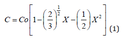
representing the expression of the boron diffusion profile after diffusion from non-oxidizing sources (D=Do(C/Co)), which shows that the concentration becomes null for the finite value Xo= √(2/3), and
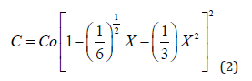
representing the expression of the boron diffusion profile after diffusion from oxidizing sources (D=Do(C/Co1/2)), which shows that the concentration becomes null for Xo=√(3/2). Following the same procedure, a general expression representing a very good approximated solution (error < 1% for m>1/2) of the diffusion equation, for the diffusion coefficient of the form D=Do(C/Co)m, where m is a real number, can be written as following [32]:
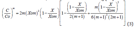
where Xom is the depth into the silicon bulk for which the impurity concentration is null, and is calculable for the condition C(X=0) =Co. As it can be seen from rel. (1), the condition C=0 for X=Xom, is automatically fulfilled.
A very interesting and useful solution of the diffusion equation for a diffusion with D on the same general form (D=Do(C/Co)m) can be obtained expressing X as a function of C, under the form [32]:
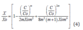
which has the advantage of a direct calculation of the diffusion depth (or junction) as geometrical parametr, useful not only for the MEMS design and fabrication, but also in any other application in microelectronics/microsystem technology for micro-devices fabrication. As in the precedent case, this form complies with the condition of C=0 for X=Xom, and this limit value is calculable from the condition X=0 for C=Co.
The analytical solutions given here for the first time, which represent solutions of the complex problem of the diffusion equation with a diffusion coefficient of the form D=Do(C/Co)m, either expressing the concentration as a function of the diffusion depth, or the diffusion depth as a func6tion of concentration – relations (3) and (4), are therefore a powerful tool for the adequate/accurate design and control processes in a large domain of the microelectronics and microsystems applications, taking into account that the diffusion of practically all of the used impurities in silicon are concentration dependent [7,8].
The analytical results presented above can be used for the calculation of the etching rate during the etching process, usually performed in alkaline (KOH, NaOH, LiOH) or of EDP solutions, which depend on the boron concentration C according to the following relation [33]:
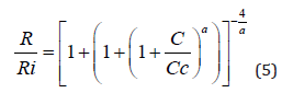
where “a” is a shape parameter, a=4 for 10% KOH (NaOH, LiOH) and ethylene-diamine-based (EDP) and a=2 for 24% alkaline solutions, while Ri is the reference (constant) etching rate of the lowdoped silicon substrate, and Cc is a specific value (2-4) ×1019 cm-3, which depends on the etching temperature and on the concentration of the solution. Similarly with the previous approach of the chemical etching of the boron-implanted layers [34], the etching time t necessary to etch the boron-doped layers after diffusion of oxidizing or non-oxidizing sources as a function of the depth x into the silicon, can be calculated from the expression:
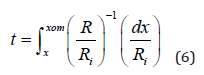
where R is expressed by the relation (5). For calculation, the
suitable expression (m=1, m=1/2) discussed above and the required
values a=2 or a=4, depending on the used solution, are to be used. Cc
can be calculated from the relation: Cc = 5.5 x 10¹⁹ exp (-0.025eV/
(kToK)) cm-3, obtained by a fitting procedure [18] of the experimental
data previously reported [33].
Therefore, the final form allowing to calculate the necessary
etching time is:
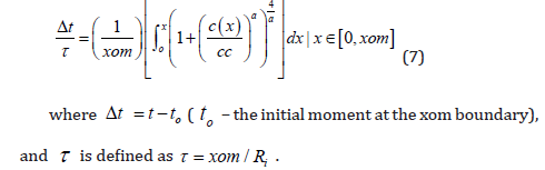
The relation (7) is useful not only to calculate the etching time to obtain the necessary thickness from the geometrical point of view, but also to eliminate the layer where the variation of boron concentration could induce undesirable mechanical stress into membrane. Comparatively, the boron diffusion from BN non-oxidizing sources shows a lower variation of concentration (like a “plateau”) near the surface of silicon [26] than that after diffusion from oxidizing sources [35,36]. A method to diminish the intrinsic tensile stress induced in the silicon lattice and thus in the silicon membrane due to the mismatch between the the boron and silicon atoms, is to dope this layer also with germanium atoms [13]. The reduction/elimination of the intrinsic stress allows the improvement of the sensor sensitivity. The fabrication of miniature silicon capacitive sensors is suitable for further integration in telemetric microelectronic systems, with advanced application in the real-time automatic measurements of the local blood pressure in biomedicine. The induction technique previously presented [13] is inherently a low-power consumption, offering a continuous availability of power through induction. The obtained results are suitable to be applied in any other design/ fabrication process of microelectromechanical structures by BMM technology. By using such results for various conditions of experiment, concerning the boron diffusion (time, temperature, nature of source) and etching processes (concentration of solution, temperature [33]), can be obtained various sets of curves under various diffusion/ etching conditions, for practical purposes of application [35,36].
The critical process of the boron diffusion in silicon for the design/fabrication of the MEMS/silicon capacitive sensors with biomedical applications was analyzed in terms of nature of sources, diffusion mechanisms and diffusion profile, showing that due to the contribution of the silicon self-interstitials to the diffusion process from oxidizing (BBr3, B2O3) sources, a dependence D=Do(C/Co)1/2 is obtained, while after diffusion from non-oxidizing BN sources, a diffusion mechanism by mono-charged vacancies is operative, which determines a typical dependence D=Do(C/Co). In order to simulate such diffusion profiles, there were deduced in each case adequate solutions of the diffusion equations as analytical forms, and a general form of such solutions for D=Do(C/Co)m (with m a real number) was given, allowing the calculation of the concentration as a function of the depth and reversely, which can be applied not only for the design/fabrication of the silicon capacitive sensors for biomedical applications, but also for other microelectronic/microsystem devices performed by silicon planar technology.
The analytical results are used for the calculation/simulation of the etching rate and time for the design/fabrication of the silicon capacitive sensors with biomedical applications by BMM technique but can be also used for other micro-mechanical MEMS elements and structures. The analytical results presented in this paper allow also to control the reduction of the stress induced by the boron concentration gradients, while the intrinsic tensile stress due to the mismatch of the silicon/boron atoms radius can be reduced by co-diffusion/doping with germanium atoms. Diffusion from BN sources show lower gradients of the profile near the silicon sources, with beneficial effect for a lower induced stress in the silicon membrane after diffusion from such sources. The micro-devices fabricated by BMM are suitable for further integration in telematics lines, with beneficial effects for real-time measurement and data processing, and for low power consumption. The presented results could be applied to any other MEMS structures or micromechanical elements, fabricated by BMM technology.
Special thanks to this Journal for the kind invitation and professional publication.