 Review Article
Introduction
Interest is currently growing in simple process to manufacture gas sensors for applications such as exhaust gas sensors in the automotive industry, monitoring furnace installations as security and environmental protection. Among the many applications of gas sensors, the production of portable systems and the need and development of multifunctional sensor systems (“electronic nose”) by means of pattern recognition method require cheap sensor devices with low power consumption. The improvement of thin film gas sensors based on semiconducting metal oxides appears in this context as a possible answer, due to the full compatibility of the modern deposition techniques with microelectronic technology.
Pd Coatings on Oxygen Sensors of TiO2 Thin Films
The high-quality performance of oxygen sensors for temperatures ranging between 100 and 500 °C can be usefully realized on the starting point of appropriate metal-oxide semiconductors [1]. On the other hand, since the observation that the adsorption of gas molecules on the surface of metal-oxide semiconductors produces a significant change in their electrical resistance, there has been a sustained effort to use this property for purposes of oxygen detection. Gas sensors based on metaloxides semiconductors have aroused relevant interest owing to high sensitivity to pollutant gases, low cost, easy implementation and small size. Among them, titanium dioxide has been put under consideration due to its good chemical stability at high temperatures and in abrasive environments beside its gas sensing feasibilities [2,3]. Titanium oxide is a native oxygen-deficient metaloxide containing donor-like oxygen vacancies and therefore is an n-type semiconductor [4]. It has three different crystalline phases: brookite (orthorhombic), anatase and rutile (both tetragonal) [5]. Rutile is a thermodynamically stable phase, while anatase and brookite irreversibly transform to rutile at high temperatures [1]. TiO2 (rutile in most cases) is used for gas sensors (hydrogen, oxygen, etc.) working at temperatures as high as 800 °C [6]. Conversely, anatase is less dense and less stable than rutile. Thin films of TiO2 anatase have been reported using the ultrasonic spray pyrolysis technique [7]. Oxygen molecules adsorbing or reacting on metal-oxide semiconductor surface create an observable change in the surface resistivity. As a result, metal-oxide semiconductors materials, such as TiO2, are often used as gas sensors by monitoring changes in the surface electrical resistivity in presence of oxygen molecules. The deposition of catalysts on the semi-conducting metal oxide surfaces has been reported to improve the sensing performance in many studies [8, 9].
The use of catalytic additives to improve the characteristics of gas sensors based on metal-oxide semiconductors is a widely extended practice in both commercial and research fields. Primary interest falls on increasing the efficiency of the introduced element to interact with the gaseous medium. Consequently, additives are introduced seeking an increase of the sensing layer selectivity and sensitivity, even at milder operation conditions. In this work, it is explored the gas sensing properties of the TiO2 anatase phase. TiO2 thin films with well characterized anatase structure have been used in gas sensitivity measurements. At relatively low temperatures (375 ≤ T ≤ 425 °C) and without palladium coatings, anatase thin films have a significant and very rapid response to oxygen. Adding anatase thin films with palladium coating (thicknesses of 20, 40, 60, and 80 Å), makes them sensitive to oxygen and modifies the response speed and characteristics. Nevertheless, only few groups report on the systematic way, of introducing a catalyst in coating form on sensitive material of the oxygen sensor device. The experiments reported in this work have been carried out as a fundamental study on the physical properties of TiO2 based samples deposited by an inexpensive ultrasonic spray pyrolysis technique [7], in order to explore their potentials in the development of the oxygen sensors devices and as a practical alternative to expensive solid state electronic gas sensor devices.
Fabrication of TiO₂ Films
Ultrasonic spray pyrolysis constitutes a versatile technique able to produce nanoscale size powders and thin films. The particle size within these powders could be easily controlled by varying the concentration of the source solution and the atomization parameters. Titanium dioxide (TiO2-anatase phase) thin films were deposited using ultrasonic spray pyrolysis technique, (Figure 1 & Figure 7). The starting solution was prepared by dissolving titanium (IV) oxide acetylacetonate [TiO [CH3COH=C(O-)CH3]2] (from Aldrich) in pure methyl alcohol [CH3OH] (from Baker) at 0.05 M concentration. The deposition system used contains a piezoelectric transducer with variable frequency, in this case set up at 1.2 MHz, and an ultrasonic power of 120 W, using a substrate temperature (Ts) of 450 °C within an accuracy of ±1 °C. Filtered air was used as carried and director gas, with air flow rates of 3.5 and 0.5 l min-1, respectively. The deposition time was 7 min. Alumina (Al2O3) substrates (sized 1.25 cm x 1.25 cm) were used to produce the oxygen sensing devices and to electrically characterize these at measurement temperatures between 100 and 500 °C. The cleansing procedure for these substrates is briefly explained: five minutes in a trichloroethylene [ClCH=CCl2] (from Baker) ultrasonic bath to degrease the substrate, followed by five minutes in a methyl alcohol and then by five minutes in an acetone [CH3COCH3] (from Baker) ultrasonic bath. The substrates were subsequently dried by blowing them with pure, dry nitrogen gas (N2) (from PRAXAIR).
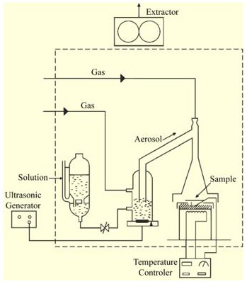
Figure 1: A schematic diagram of influenza A virus.
Incorporation of Pd Coatings on TiO₂ Thin Films and Fabrication of The Oxygen sensors
The purpose of incorporating palladium coatings in the metaloxide semiconductor is to increase the velocity of the chemical reaction during which the gas detection takes place. This is reflected in the electrical properties by increasing the sensitivity of the oxygen. Palladium coatings were incorporated on the TiO2-anatase phase thin film surface according to the following procedure. First, gas sensors were produced using optimal preparation conditions for the TiO2-anatase phase thin films to this end. Interdigital electrodes were deposited on Alumina (Al2O3) substrates, previously washed through vacuum thermal evaporation of gold (Au) [wire, 0.5 mm diam., 99.999% (from Aldrich)] through a metallic mask. This was done in order to obtain a maximum specific area (surface area/ volume ratio), which resulted in a spacing between the electrode fingers of approximately 1.1 mm with electrodes having a thickness of 1.5 μm. Afterwards, using ultrasonic spray pyrolysis, TiO2-anatase phase thin films were deposited through a stainless-steel mask on the interdigital electrodes. Palladium [wire, 0.5 mm diam., 99.99% (from Aldrich)] coatings were deposited through a metallic mask by thermal vacuum evaporation to obtain Pd coatings thicknesses of 20, 40, 60, and 80 Å, which were measured in situ with a quartz crystal thickness measurement device.
Oxygen Sensor Characterization
Oxygen sensor, Figure 2 (a), characterization was carried out by placing the sensors in a sample-holder placed into a measurement chamber with a vacuum capacity of 10-6 Torr. The measurement chamber simultaneously allowed the introduction of different gases in a controlled way. The schematics of the characterization system are shown in Figure 2 (b). The ambient gas under consideration was zero-grade air [Composition: O2 19.5 - 23.5 %, H2O < 3 ppm, CO2 < 3 ppm, (Total Hydrocarbon Content) THC < 1ppm] (from PRAXAIR) and the gas being detected was oxygen (O2) (from PRAXAIR). Using a LENOX LASER flux control in the valves, gas concentration in the ambient gas atmosphere was controlled. Sensor characterization was performed by measuring the change in the electrical resistance (DR) of the active film as a result of its interaction with the O2 being detected. This change in the electrical resistance was measured as a function of two main parameters:
a) Temperature variations during measurements, under a given ambient gas concentration, which allowed the determination of the optimal operating temperature sensor, and
b) Variations on O2 concentration at constant temperature during measurement, which allowed an adequate determination of the sensor sensitivity (s).
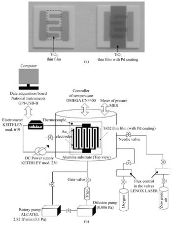
Figure 2: (a-b) Photographs of the oxygen sensor devices. (c) Schematic diagram of the system used to measure electrical properties in controlled atmospheres and temperatures. L. Castañeda. et al.
Last parameter can be adequately expressed as a function of the relative difference of resistances with respect to O2 concentration in the following way: s = (Rgas - R0)/R0, i.e., the minimum concentration of the detected O2 at which the sensor exhibits an appreciable response. In both cases, changes in the electrical resistance of the active film as a function of the exposition time to the gas mixture were measured, and after stabilization a constant value or a saturation value was reached. It is noteworthy that the response time of a sensor is defined as the required time to reach 90% of its saturation value (in the present case, for the DR parameter). Once this process was achieved, the detected gas was removed from the ambient atmosphere in a sudden way to determine the reversibility of the detection process. If the detection process shows reversibility, then the electrical resistance of the active layer will exhibit the same value it had before oxygen exposition.
Figure 3(a) shows the variation of the electrical resistance of a sensor device with a 220 nm thick titanium dioxide film, deposited at a substrate temperature of 450 °C and measurement temperature of 400 °C, as a function of exposition time for two excess oxygen concentrations. The O2 concentrations in the measurement chamber were set to values of 1,000 and 10,000 pp. Typical curves for gas sensing devices are observed for these experimental conditions, in which the action of the oxygen gas provokes an increment in the electrical resistance of the active film. Therefore, this graph serves as a proof of the use of TiO2 thin films, elaborated through ultrasonic spray pyrolysis, as adequate O2 detectors, at least for a concentration range of 1,000 to 10,000 ppm. Similar curves are obtained for each device prepared, once the corresponding temperature and oxygen concentrations of the atmosphere are adequately established. The general shape of the shown curves can be explained by considering that the titanium dioxide surface (active film) contains a number of oxygen-related physisorption’s and chemisorption’s species, being the main ones: H2O, OH-, O2, O2-, and O-. From these, the more predominant species are O2- and O-. It is worthwhile mentioning that the presence of these species modifies the electrical behavior of the active layer, since both of these dominant species are negatively ionized when adsorbed onto the oxide surface, indicating they have captured an electron from the lattice, which in turn increases the electrical resistance of the sensor. Expressions (1.1) and (1.2) show the chemical reactions leading to the production of these ionized species:


Under the action of an oxidizing gas, the mixture acquires electrons from the oxide because it is at that temperature that the concentration of the ionized species O2- and O-, coming from molecular oxygen (O2), is increased. This results in a greater electrical resistance.
Sensitivity variations as a function of the measurement temperature are shown in Figure 3(b). In this case, sensitivity was calculated for O2 concentrations of 1,000 and 10,000 ppm in zerograde air. Figure 3(b) also shows that temperature is a catalyzing factor for oxygen adsorption, a fact that is manifested in the initial portion of the graph through an increased sensitivity as temperature rises, until a maximum value is achieved. This temperature, at which a maximum measurement is obtained, is considered to be the optimal device operation temperature. In a similar fashion, measurements were made for temperatures ranging from 100 to 500 °C in 50 °C steps with a 10,000 ppm O2 excess concentration in zero-grade air in order to determine the optimal operation temperature of the gas sensors. The sensitivity behavior displayed in Figure 3 (b) must be understood by taking the definition of sensitivity into consideration. On the other hand, an increment in the gas sensor sensitivity as a function of the O2 excess concentration is observed when the temperature of the sensor remains constant. This particular behavior can be accounted for by considering that having greater molecular oxygen concentration in the atmosphere, also produces a greater number of O2- and O- species. This takes placesbecause the adsorption of molecular oxygen on the titanium dioxide surface (i.e., the active film) contributes to the production of O2- species; and when this particle decomposes, it produces Ospecies. Since both of these clearly dominant species are negatively ionized after acquiring an electron from the oxide, an increment in the electrical resistance is observed. Thus, the presence of these species modifies the electrical behavior of the active layer.
Gas sensor response time was directly obtained from the measurements of variations in electrical resistance as a function of exposure time under a given set of atmosphere and temperature conditions, that is, curves similar to those shown in Figure 3(a) for each case. The mean response time of the oxygen sensor, at a temperature of 400 °C when 120 to 10,000 ppm oxygen excess concentrations were used, was about 70 seconds on average. Interestingly enough, the average recuperation time for the oxygen sensors for identical oxygen excess concentrations and operation temperature conditions was in the order of 1800 seconds. The incorporation of palladium as a catalyst was realized through vacuum thermal evaporation, depositing coatings of 20, 40, 60, and 80 Å thicknesses through a metal mask. Figure 4(a) displays the behavior of electrical resistance of a device using palladium as a catalyst in a film with a thickness of 80Å, as a function of the oxygen concentration for a measurement temperature of 300 °C and a TiO2 film thickness of 220 nm. O2 concentrations were established at 100, 200, 800, and 1,000 ppm. Once again, the behavior observed in all measurement conditions presents the typical expected response for this type of devices. Figure 4(b) shows the sensitivity variation as a function of measurement temperature in the case of TiO2 thin films on which a palladium thin film was deposited. As was mentioned above the film thickness of the palladium coating was varied. The Figure 4 (b) illustrates that maximum sensitivity is obtained for a palladium film with a thickness of 80 Å. The sensitivity behavior with the palladium thickness is related to the magnitude of the surface area for catalytic activity. This result can be explained considering that the thickness of the palladium films did not enable these to be continuous, thereby implying that those with lesser thicknesses could be formed by palladium “islands” on the surface of the titanium dioxide [10,11]. Since the general shape of these curves is similar to the one shown by the corresponding figures obtained for other catalysts, the explanation of the observed behavior is the same.
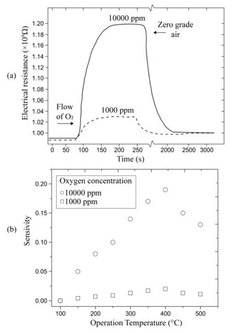
Figure 3:
(a) Electrical resistance variation as a function of time, considering different input flux concentrations of O2 in zero-degree air at a temperature of 400 °C.
(b) Sensitivity variation as a function of temperature for different concentrations of O2 influxes in zero-degree air.L. Castañeda. et al.
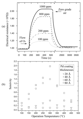
Figure 4:
a) Variations in electrical resistance as a function of exposure time for a Pd catalyst device (thermal evaporation with 80 Å thickness) for different O2 concentrations in zero-degree air at 300 °C.
b) Sensitivity variation of a gas sensor based on the incorporation of Pd as a catalyst (in different thicknesses), as a function of temperature for a 1,000 ppm of O2 diluted in zero-degree air.L. Castañeda. et al.
For the case of the 40 Å palladium coating in which sensitivity decreases, the result could be explained arguing that a greater uniformity exists in the Pd coating. This results in a lower catalyst surface area because the kinetics of the catalyzed heterogeneous reaction occurring at an atomic or molecular scale affects its activity.
TiO2 Thin Films Using Rh, Ni and Ir as Catalyst
In this section we explore the gas sensing properties of the anatase phase TiO2 thin films. Un-doped TiO2 thin films with wellcharacterized anatase structure present a significant and very rapid response to oxygen at relatively low temperatures (375≤T≤425 ◦C). The addition of catalysts such as iridium, nickel, and rhodium to the TiO2 films makes them more sensitive to oxygen and modifies the response speed. The catalytic effect of these elements is based on their work function values, which are higher than the ZnO work function. Then, when a catalyst is present on the surface region, an accumulation of electrons will be generated along that region, which will increase the adsorption of different oxygen species, and consequently the surface resistance will increase.
Incorporation of Catalysts
TiO2 thin films from Figure 2 (b), were deposited through a stainless-steel mask on the electrode’s region by the USP technique, leaving free from TiO2 deposition the two main bars. USP technique constitutes a versatile technique able to produce nanoscale size powders and thin films. The particle size within these powders could be easily controlled by varying the concentration of the source solution and the atomization parameters. A schematic diagram of the USP system used is shown in Figure 1. The starting solution was prepared by dissolving titanium (IV) oxide acetylacetonate (TiO(CH3COH= C(O−)CH3)2, Aldrich) in pure methyl alcohol(CH3OH, Baker) at a 0.05M concentration. The deposition system used contains a piezoelectric transducer operating at variable frequency, which was set to 1.2 MHz, and an ultrasonic power of 120W, using a substrate temperature (Ts) of 450◦C within an accuracy of±1 OC. Filtered atmospheric air was used as carrier and director gas, with air flow rates of 3.5 and 0.5 lmin−1, respectively, within an accuracy of ±0.05 lmin−1. The deposition time was set to 7.0min. Firstly, un-doped TiO2 films with a thickness in the order of 220nm were produced under optimal preparation conditions in order to have a reference for comparison of the characterization results. Secondly, catalysts were added to these. The catalysts (Ir, Ni,and Rh) were incorporated on the surface of the active TiO2 film by two different methods. The first one consists in the impregnation of the TiO2 thin films, previously deposited on the alumina substrates, from a chemical solution containing the particular catalyst. The starting solutions containing the different catalysts were separately prepared maintaining a fix concentration at 1.55×10⁻⁴Mof, iridium (III) acetylacetonate ((CH3COCH= C(O−)CH3)3Ir), nickel (II) acetylacetonate (Ni(C5H7O2)2), and rhodium (III) acetylacetonate ((CH3COCH= C(O−)CH3)3Rh), all of them from Aldrich. The TiO2films were impregnated with the respective solutions by applying hundreds of brushstrokes by the “paint on” method, using a brush, and since the solvent in which the catalysts were suspended is evaporated at 475 ◦C, the films were annealed at this temperature in atmospheric air for 1 h.
The second method consists in the USP of the different starting solutions (the same used in the impregnation method) on the TiO2thin films. The deposition conditions were similar to those used for spraying the TiO2 thin films with the exception of the substrate temperature, which was 475 ◦C, within an accuracy of ±1 ◦C, in this case. It is from this temperature on that the thermogravimetric analysis shows a loss of mass of the organic part of the compound. Figure 5 (a) shows the iridium (III) acetylacetonate TG analysis, which is quite similar to the rhodium (III) acetylacetonate. Figure 5 (b) shows the nickel (II) acetylacetonate TG curve. The TG characterization was performed using a DUPONT model 951- TG thermo-gravimetric analyzer. The catalyst concentration incorporated on the TiO2 thin film surface was determined using energy dispersive spectroscopy (EDS). The equipment was a Joel JSM 5200 scanning electron microscope (SEM), equipped with an EDS X-ray detector having a 60 resolution.
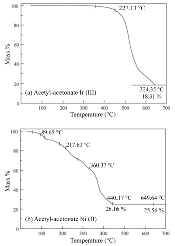
Figure 5: Thermo-gravimetric analysis of
(a) Iridium (III) acetylacetonate and
(b) Nickel (II) acetylacetonate.L. Castañeda. et al.
Characterization of the Gas Sensor
Gas sensor characterization was carried out in a sample-holder placed into a measurement chamber with a vacuum capacity of 10−6 Torr, Figure 2 (c). The measurement chamber simultaneously allowed the introduction of different gases in a controlled way. The electrical conductivity response was measured by monitoring the DC current under constant bias voltage of 5 V, by using a DC power supply (Keithley model 230), and an electrometer (Keithley, model 619). At this bias voltage the current–voltagebehaviorwas ohmic. A diagramof the characterization system is shown in Figure 2 (c). The sensing properties were determined in an oxidant atmosphere consistingin oxygen (Praxair) mixed in zero-grade air (Praxair) (composition: O2 = 19.5–23.5%, H2O< 3 ppm, CO2 < 3 ppm, total hydrocarbon content (THC) < 1 ppm). Using a LENOX LASER flux control in the valves,gas concentration in the ambient gas atmosphere was controlled. Sensor characterization was performed by measuring thechange in the electrical resistance (R) of the film as a result ofits interaction with the detecting gas. This change in the electricalresistance was measured as a function of two main parameters:
a) operation temperature and
b) oxygen concentration in the atmosphere.
The parameter that gives information about the sensing properties, which is a direct function of the resistance change, is the sensor response, defined as s = (R_gas - R_0)/R_0, where Rgas and R0 are the thin film resistance measured in oxygen and zero grade air, respectively, i.e. the minimum concentration of the detected O2 at which the sensor exhibits an appreciable response.
In both cases, changes in the electrical resistance of the active film as a function of the exposition time to the gas mixture were measured, and after stabilization a constant value or a saturation value was reached. It is noteworthy that the response time of a sensor is defined as the required time to reach 90 % of its saturation value (in the present case, for the ΔR parameter). Once this process was achieved, the detected gas was removed from the ambient atmosphere in a sudden way (in other terms, the valve of oxygen was closed, approximately in 1 s) to determine the reversibility of the detection process. If the detection process shows reversibility, then the electrical resistance of the active layer will exhibit the same value it had before oxygen exposition. It is well-known that the operation temperature is a catalyzing factor in gas sensors. In order to determine the optimal temperature of our sensors, variation in response of a device with a 220nmthick titanium dioxide film was obtained as a function of the operation temperature. Measurements were made at temperatures ranging from 100 to 500 ◦C at a 50◦C step in an atmosphere containing 1000 and 10,000ppm of O2 diluted in zero-grade air (Figure 6). An increasing oxygen adsorption is manifested by the response behavior as temperature increases, until a maximum value is achieved. This temperature, at which a maximum response is obtained, is considered to be the optimal device operation temperature. The response behavior displayed in Figure 6 must be understood by taking the definition of response into consideration. On the other hand, an increment in the sensor response as a function of the O2 excess concentration is observed when the temperature remains constant. This particular behavior can be accounted for considering that having greater molecular oxygen concentration in the atmosphere also produces a greater number of O2 − and O− species.
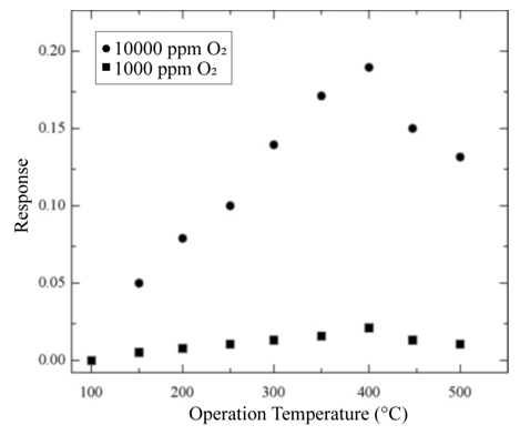
Figure 6: Variation in response of a TiO2 film as a function of operationtemperature, for two different concentrations of O2 influxes (1000 and 10,000 ppm) diluted in zero-grade air.L. Castañeda. et al.
This takes place because the adsorption of molecular oxygen on the titanium dioxide surface (i.e., the active thin film) contributes to the production of O2 − species, and when this particle decomposes, it produces O− species. Since both of these clearly dominant species are negatively ionized after acquiring an electron from the oxide, an increment in the electrical resistance is registered. Thus, the presence of these species modifies the electrical behavior of the active layer. Additionally, four regions with different behavior can be noticed in Figure 6. The existence of each of these is related to the type and quantity of the oxygen species adsorbed, which are also a function of the measurement temperature. A detailed explanation of each region is listed below.
First Region
This region starts at room temperature (∼= 23 ◦C) and ends at 100 ◦C. No variations in response were observed, since this temperature interval only allows the adsorption of O2 − on the surface through the chemical reaction described by Eq. (2), which requires relatively low energy to enable its formation and manifests itself in small concentrations. At 100 ◦C, O− species are formed and are dominantly present [12].

Second Region
It is situated in the 100–225 ◦C temperature interval. As previously mentioned, the O− species start to appear at 100 ◦C in a dominant way and with greater concentration than theO2 − species. This provokes an increment in the response variation, as can be seen in Figure 6. It is precisely in this region that the greatest increment in sensitivity is displayed. The chemical reaction taking place in this temperature interval is described by the following equation:

Third Region
This region is located between 225 and 400 ◦C. Response variations, in almost all cases, show a slight decrease in the increment rate, even when the available thermal energy is enough to adsorb all three types of possible oxygen species, namely O2 −, O−, and O2−. The O2− species is produced through the chemical reaction expressed by the following equation:

Nevertheless, the number of available sites in the surface for adsorption is small and it decreases each time, and consequently the probability of charge desertion increases. Therefore, the change in resistance starts decreasing and is obtained a maximum value when it reaches 400 ◦C, i.e., the so-called “optimal operation temperature”.
Fourth Region
This region is present for operation temperatures above 400 ◦C. Clearly, the conditions under which the maximum response value is obtained are also those for which the maximum value of the titanium dioxide thin film resistance is measured. This indicates that the oxidation reactions described by Eqs. (1.3)–(1.5) can no longer occur since there are no more available sites on the surface. However, this does not justify that beyond 400 ◦C a decrease in response is observed. Consequently, this behavior is related to the probability of an increase in the desorption of other species, which in turn decreases the number of chemical reactions in which electrons are reacquired by the active layer as well as the magnitude of the electrical resistance. Resistances for operation temperatures above 500◦C were not regularlymeasured, mainly because there was no particular need for this, as the majority of the “interesting” phenomena occur at lower temperatures. Response time of these sensors, shown in Figure 9, was directly obtained from the measurements of electrical resistance as a function of exposure time under atmosphere and temperature conditions constant. The mean response time for single TiO2 films at a temperature of 400 ◦C when 1000–10,000ppm oxygen excess concentrations were used was about 70 s on average. Interestingly enough, the average recovery time for the oxygen sensors for identical oxygen excess concentrations and operation temperature conditions was in the order of 30 min.
A typical response for gas sensing devices, in which the action of the oxidant gas being detected provokes an increment in the electrical resistance of the active film, can be observed. Therefore, this graph serves as a proof of the use of TiO2 thin films, elaborated through USP, as adequate oxygen detectors, at least for a concentration range of 1000–10,000 ppm. Similar curves are obtained in all the devices prepared, once the corresponding operation temperature and oxygen concentrations of the atmosphere are adequately established. Once the single TiO2 films were characterized the catalysts were incorporated to the films. Figure 8 (a) and b shows the typical energy dispersion analysis spectra of samples using Ni as a catalyzing element and incorporated by USP and impregnation, respectively. Similar spectra were obtained for other elements used as a catalyst, namely, iridium and rhodium. A qualitative analysis was performed from these spectra to identify the elements present in the samples. Using a computer program routine, the positions of the spectral peaks were determined and compared with the tabulated values of the X-ray energy emissions. A quantitative analysis was then carried out in order to reveal the concentrations of the elements present in the samples. Figure 8 (a) shows peaks located at different energy levels related to titanium and nickel. Caution must be placed on the fact that the EDS technique does not allow oxygen detection. The concentration of these metals is shown in Table 1. Concentrations of iridium and rhodium in the samples prepared by USP and impregnation are also shown in Table 1.
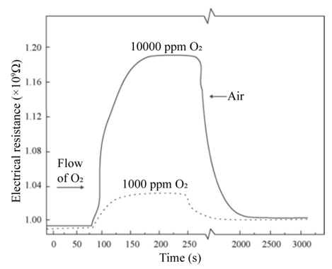
Figure 7: Electrical resistance variation as a function of time, considering two different input flux concentrations of O2 in zerograde air at a temperature of 400 0C.L. Castañeda. et al.
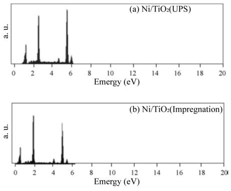
Figure 8: Typical spectrum obtained in Ni/TiO2 samples through energy dispersion analysis.
a) Ni incorporated by USP on the TiO2 thin film.
b) Ni incorporated through the impregnation in the solution of the TiO2 thin film.L. Castañeda. et al.
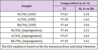
Table 1: Results of EDS analysis of TiO2 samples with three different metal catalysts loadedby USP and impregnation methods.
The EDS spectrum of the Ni-impregnated sample in Figure 8 (b) shows similar peaks to Figure 8 (a) in practically identical locations. The catalyst concentrations incorporated in all the characterized TiO2 films are of the same level (∼= 2.5 at.%).The variation in response of TiO2 films with nickel incorporated by both methods is shown as a function of the measurement temperature in Figure 9 (a). These measurements were made in an atmosphere containing an O2 excess concentration of 10,000ppm in zero-grade air. As can be observed, the response presents a temperature dependence similar to the devices without catalysts (Figure 6). This is, the response rises as the temperature increases until a maximum is reached, after which it continuously decreases. This figure displays the typical behavior obtained for the response variations as a function of sensor temperature. On the other hand, the magnitude of response depends on the procedure used to incorporate the catalyst, and a far larger sensitivity than in device lacking the nickel catalyst is obtained. Figure 9 (c) and c show the responses as a function of measurement temperature for the samples containing Ir and Rh, respectively. Once again, an excess concentration of O2 with 10,000ppm in zero grade air was used. Both figures show, in a general way, the same typical behavior, and the magnitude of response is also dependent on the procedure to incorporate the catalyst elements. Nevertheless, in the case of the films containing Ir as a catalyst, the response takes on larger values. The response values obtained for the particular case of USP are unexpectedly small in comparison with the sample using Ni as a catalyst.
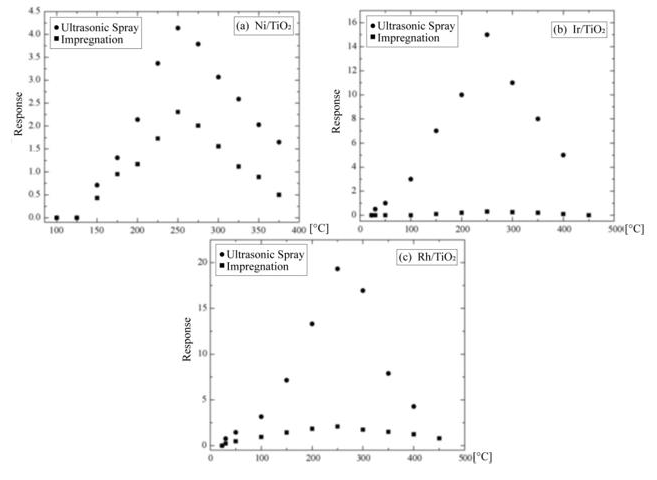
Figure 9: Variation in response of gas sensors with catalysts as a function of temperature to a 10,000ppm of O2 diluted in zerograde air.
(a) Ni/TiO2
(b) Ir/TiO2, and
(c) Rh/TiO2. L. Castañeda. et al.
In general, irrespective of the catalyst, the response magnitude is greater when the procedure to incorporate the catalyst elements is impregnation. Accordingly, this suggests that such procedure enable obtaining a more uniform distribution with a greater degree of layer covering on the surface of the active film, which results in an extension of the surface area of the catalyst since the process takes place in an atomic or molecular scale.
In the case when the starting solution is sprayed onto the TiO2 film, two effects may be achieved. (i) Although using organometallic materials as a source of catalysts have relatively low decomposition temperatures (<300 ◦C), the incorporation process of these catalysts takes place through the direct incidence of the spray droplets on the surface of the active film, resulting in a lower degree of layer protection, and a lower extension of the surface area. (ii) Due to the substrate temperature of 475 ◦C during the spraying, if the incorporation process is in an atomic or molecular level and having a relatively high substrate temperature, the radicals related to the catalyst element (Ni, Ir, and Rh), which are adsorbed, have a higher surface mobility, which enables to travel longer paths before equilibrating with the substrate surface, in turn generating nuclei growth. Nevertheless, since the concentration of the solution is extremely small, the growth of these nuclei does not continue, and the surface area of the catalyst is minor. Furthermore, among other factors, catalyst activity heavily depends on the extension of surface area [13,14]. The importance of this variable in catalytic activity is clearly notable through the difference in the response magnitudes observed when the catalyst incorporation procedures vary. In a general way, O2 gas sensors based on the incorporation of catalysts on thesurface of TiO2 films may be examined in accordance with the following reaction between the molecular oxygen and the catalyst:

where M(s)• is the transition metal (catalyst). Molecular oxygen coming on the catalyst is thus dissociated as a result, forming ionic bonds between the catalyst and the oxygen. Atomic oxygen produced in this way migrates on the surface of the material, where the following reaction takes place:

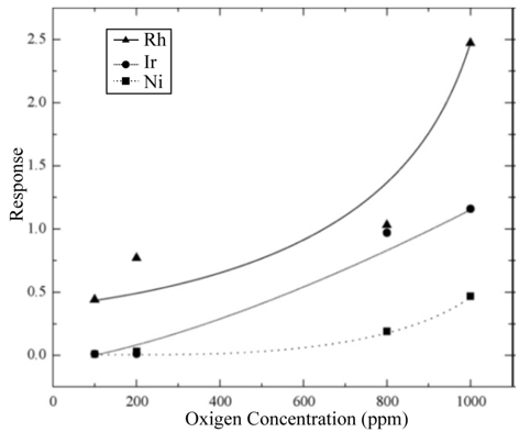
Figure 10: Variation in response of the gas sensing devices with impregnated catalysts as a function of oxygen concentration measured at 250 0C.L. Castañeda. et al.
In the chemical reaction described by Eq. (6), the atomic oxygen, generated through the action of the catalyst on the molecular oxygen, adsorbs an electron from the active TiO2 film, becoming negatively ionized. This removal of electrons from the surface of the active film creates a surface layer with a conducting electron concentration smaller than in the bulk, thereby producing an increment in the electrical resistance of the TiO2 surface. In general, the action of a catalyst incorporated on the surface of the active layer formed by a polycrystalline material is considered in the following way: the catalyst increases the response speed as well as the response magnitude of the gas sensors. Sensor operation temperature is likewise reduced as is shown in Figure 8 (a–c) in comparison with results shown in Figure 6. This result is linked to the fact that molecular oxygen dissociation requires less energy to take place due to the catalyst action. Figure 10 displays the response values of the devices with catalysts incorporated by impregnation as a function of the excess oxygen concentration, from 100 to 1000 ppm, at an operation temperature of 250 ◦C. The response rises when the oxygen concentration increases, a fact to be expected, since the oxygen sensor response is explained by the adsorption of oxygen species. At this operation temperature (250 ◦C), and due to the interaction with the catalyst, atomic oxygen is formed, resulting in a greater number of negative oxygen ions adsorbed and leading to a greater electrical resistance change. In general, the curves shown in Figure 10 display a tendency towards a maximum response value for greater oxygen concentrations in the ambient atmosphere.
ZnO:Ru Thin Solid Films Deposited by The Sol-Gel Technique
ZnO is an “n-type” wide band gap AIIBVI semiconductor with hexagonal wurtzite structure (space group (C63mc)) with lattice parameters of a = 0.3296, and c = 0.52065 nm [15]. It is believed that the “n-type” conductivity observed in this material is mainly due to both zinc excess located in interstitial positions, and oxygen vacancies, although the discussion on the origin of the intrinsic conductivity type is controversial [16]. The high transparency (>80%) in the visible region, and the refractive index magnitude (1.7 - 2.0) of ZnO thin solid films, together with their low electrical resistivity allow their application as antireflective coatings, conductive electrodes, window layer in solar cells [17], and recently reported, as light emitting devices [18]. In addition, the variation of the surface resistance as a consequence of the chemisorption of gases make the ZnO thin films adequate for gas sensing applications [19], whereas the piezoelectric properties observed in ZnO films with a (002) preferential growth allow its application in acoustic wave filters [20]. On the other hand, ZnO has gained substantial interest in the research community in part because of its large exciton binding energy (60 meV), which could lead to lasing action based on exciton recombination even above room-temperature. Two advantages of ZnO films over others TCO´s is the simplicity of the etching processes in microelectronics applications, and its good adherence to a wide variety of substrates.
Zinc oxide thin films have been prepared by using different techniques such as vacuum evaporation [21], sputtering [22], sol-gel [23], pulsed laser deposition (PLD) [24], pneumatic and ultrasonic spray pyrolysis [25, 26], molecular beam epitaxy (MBE) [27], and chemical vapor deposition (CVD) [28], among others. Solgel is a simple deposition technique that presents a low-cost setup, easy to handle, and can be scaled for deposition on large areas. It is worthy of note that sol-gel deposition efficiency surpasses other chemical techniques, decreasing the waste of reactants; moreover, the set-up does not require expensive vacuum system for synthesis. Hence, by the sol-gel technique, low-cost manufacturing of ZnO thin films can be guaranteed [29]. According to a thorough search in the literature, we have found that, uniform, reliable, and high quality ZnO thin films have been deposited by the sol-gel technique [29-34]; however, is usual that some authors start from metal alkoxides as reagent chemicals in the sol-gel process. In this respect, metal alkoxides are more expensive than inorganic salts and the preparation of a sol is tedious, since it is a slow process, and deposition process is highly sensitive to environmental conditions [35-40]. This is the main reason for searching simpler deposition techniques that facilitate the deposition process and the implementation of large-scale production. In this work we are presenting some results obtained from the characterization of solgel deposited ZnO thin films.
On the other hand, it is well-known that the addition of impurities or dopants to the ZnO lattice produces dramatic changes in their electrical, optical and structural characteristics. The incorporation efficiency of dopant elements depends on its electro-negativity and the ionic radius. In this respect, very successful doping of ZnO thin films with elements from groups IIIA and IIIB to obtain transparent and conductive electrodes has been reported [41-45]; in contrast the doping of ZnO films with either smaller or bigger ionic radii has been also reported as well [29]. The selection of a dopant depends on the application of the films [46]; in this respect, even though semiconductor oxides like ZnO are catalytically active, a small amount of metal catalysts are often added to improve the sensitivity and selectivity of these devices. In this work we have selected Ru as dopant, due to its work function value is adequate for this purpose (4.5-5-5 eV) [47], then we are testing the catalyst properties of Ru in ZnO films deposited by the sol-gel technique. The interest in simple processes to manufacture gas sensors for applications such as exhaust gas sensors in the automotive industry, or for monitoring furnace installations or flammable and toxic gases, is currently growing. The role of noble metals and transition elements in the operation and enhancing of gas sensors has been documented extensively [48-51], however at our best knowledge, there is a lack of information in the professional literature regarding the doping of ZnO films with Ru deposited by sol-gel for gas sensor applications.
Thin Solid Film Deposition
The ZnO:Ru thin solid films were prepared by the sol-gel method based on a non-alkoxide route. A 0.6 M solution was prepared from zinc acetate dihydrate [Zn(C2H3O2)2•2H2O] (from Alfa Aesar) dissolved in a mixture of 2 methoxyethanol [CH3OCH2CH2OH] (from Sigma-Aldrich), and monoethanolamide (MEA) [(CH2CH2OH) NH2] (from Baker) at room temperature (23 °C). The starting solution was stirred at room temperature during one hour until a homogeneous and transparent solution was obtained. Ruthenium trichloride [RuCl3] (from Alfa) was used as doping source. A [Ru]/[Zn] atomic percent ratio of 3.0 at% was used. The final solution was sealed and settled for seven days at room temperature in a dark environment before depositing the films (process defined as ageing). The ZnO:Ru films were deposited on clean soda-lime glass substrates, 2.5 cm x 2.5 cm). The following cleaning procedure was used: a five-minute washing in trichloroethylene [C2HCl3] (from Baker) to degrease the substrate, followed by five minutes in acetone [CH3COCH3] (from Baker), then five minutes in methyl alcohol [CH3OH] (from Baker), and finally, a drying under a nitrogen flow [N2] (from PRAXAIR). All washing steps were carried out in an ultrasonic water bath. Substrates were dipped into the starting solution and pulled from this, at a constant rate of 1.0 cm s-1. In order to remove the residual solvents from the coated substrates, an annealing process, in air at 260 °C for ten minutes, after each dipping-pulling step (immersion) was carried out. The selection of the annealing temperature magnitude was based on the boiling points of 2-methoxyethanol [C3H8O2] (from Baker) and monoethanolamide (MEA) [(CH2CH2OH) NH2] (from Baker), 125 and 170 °C, respectively.
In this deposition technique, the variation of the film thicknesses is reached by repeating the immersions number of the samples into the starting solution; therefore, we used 2, 3, 5, and 7 immersions. Finally, all deposited samples were thermally treated at 400 °C, in air at atmospheric pressure. The main purpose of this low-temperature annealing step is obtained an homogeneous distribution of the Ru ions in substitutional or interstitial positions into the ZnO lattice.
Thin Solid Film Analysis
Films thickness was measured by using a profilometer KLATencor P-15 (with a resolution of 0.15 nm) on a step chemically manufactured. The average magnitudes were around 150, 175, 195, and 210 nm for films deposited from 2, 3, 5, and 7 immersions, respectively, with an accuracy of 10 %. The film structure was studied by X-ray diffraction measurements by using a Siemens D5000 diffractometer with a Cu-Ka1 (l = 0.15405 nm) radiation. The surface morphology of the films was studied by Atomic Force Microscopy (AFM) (Park Auto Probe CP equipment). This analysis was performed in contact mode using a Si UltracleverTM tip with an applied force of 0.26 N m-1, and a resonant frequency of 40 kHz. The applied force on the surface was of 0.8 nN. The morphological characterization was complemented with scanning electron microscopy (SEM) developed in a JEOL JSM 5400 LV electron microscope. A LabRAM (HR) Dispersive Raman Spectrometer equipped with an Olympus microscope (BX41) was used to obtain the Raman spectra of the samples. An Olympus 100 X objective (N.A. = 0.9) was used as focusing optical system for the Raman laser source (see below); the spot size of the focused laser beam on the sample was ~28 μm2. The same objective was also implemented as collecting optical system for the backscattered light in a 180 º backscattering configuration. The scattered light was detected by a charge coupled device (CCD) detector, thermoelectrically cooled to –70 ºC. The spectrometer used a convenient optical grating (600 lines mm-1) to resolve the scattered radiation and an edge filter to block the Rayleigh light. The pinhole of the monochromatic was set at 400 μm. The Raman spectra were integrated over 3 s with a resolution of ~ 1.0 cm 1. The excitation source was a 632.8 nm radiation from a He-Ne laser, and the incident power at the sample was around 17 mW.
The Ru concentration incorporated on the ZnO thin solid films were determined using energy dispersive spectroscopy (EDS), with a JEOL JSM 5400 LV scanning electron microscopy (SEM), equipped with an EDS X-ray detector MORAN (Quest) having a 136- eV resolution. Additionally, a compositional analysis by Secondary Ion Mass Spectrometry Technique (SIMS) was developed to confirm the Ru incorporation into the ZnO lattice. The analysis was performed with a CAMECA IMS-6F Ion Microprobe equipped with a cesium ion gun and duoplasmatron ion sources. Mass resolution 300-20000 (M1/|M1-M2|), detectable elements: All elements from Hydrogen until Uranium. Dynamic Interval: 9 orders of magnitude (as a consequence it is possible to have a resolution of parts per million ppm and with the difference in ionization probability it is possible to reach parts per billion ppb). Depth profile resolution: nanometers, spacial resolution: 10 - 0.1 microns. The nonlinear optical absorption of the samples was analyzed by using an inputoutput experiment made with the second harmonic of an Nd-YAG laser source. A single beam with 532 nm wavelength and 2 ns pulse duration was employed in order to identify the nonlinear optical absorptive mechanism exhibited by the films.
The sensing properties of the ZnO:Ru films were probed by monitoring the surface resistance change in an atmosphere of propane [C3H8](from PRAXAIR) at different concentrations (0, 50, 100, 200, 300, 400, and 500 ppm) and different operation temperatures (23, 100, 200, and 300 °C) by using an experimental set-up reported in a previous work [52]. The resistance measurements were taken with a high resistance Keithley 2001 multimeter. Two linear ohmic contacts were manufactured onto the ZnO:Ru films by adhesive silver paint (Alpha-Aesar); the ohmic behavior was tested by the linearity of the current-voltaje curve, carried out in a in a Tektronix 577-177-D1 equipment. Two rigid tungsten probes were used as electrodes. The sensitivity of the films is calculated as s = (Rgas - R0)/R0where, R0 and Rgas are the surface resistances of the film measured in air and propane, respectively.
Structural Characterization
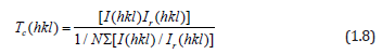
X-ray diffraction (XRD) studies have been performed to measure the crystallite sizes and texture coefficients (Tc) of the ZnO:Ru samples. The films are mainly polycrystalline, and exhibit a variety of growing crystallographic planes, mainly (002), and (103). The relative intensity of the peaks associated with such planes changes with the film thickness of the samples. In this case, a measurement of the preferential growth is the texture coefficient (Tc (h k l)) which is defined as [53]:
where I(h k l) and Ir(h k l) denote, respectively, the integrated intensities of (hkl) reflection of the textured sample and randomly oriented one and N is the number of reflections. Figure 11 shows the XRD patterns of the ZnO:Ru films with different thickness. Tc(hkl) of the films varies with the thickness or immersions number, from 1.15 to 2.34 for (002), and 0.34 to 0.67 for (103) peaks. In general, it seems from XRDanalysis that Tc(002) and Tc(103) are favored in the case of films with the biggest film thickness. X-ray spectra show a clear tendency for orientation along c axis. The mean crystallite size can be determined from the integral width β of the (002) line according to Scherer’s formula [54]:
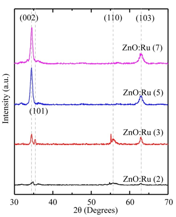
Figure 11: X-ray diffraction patterns of ZnO:Ru thin films with different film thickness, a) 2, b) 3, c) 5, and d) 7 immersions.L. Castañeda. et al.
where λ = 0.15406 nm, is the wavelength of Cu-Ka1 radiation, the correction factor k = 1.05, θ is Bragg angle diffraction with wavelength λ, B has been recorded after taking into account of instrumental broadening. The crystallite size of the samples varies from 25 to 35 nm with an accuracy of 10 %.
Micro-Raman Spectroscopy
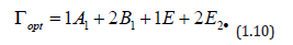
Wurtzite crystals exhibit one of the simplest uniaxial structures and hence form an important class of materials to analyze by Raman spectroscopy when fundamental processes are being investigated. Wurtzite-type ZnO belongs to the spatial group C_6v^4 (C63mc) with two formula units in the primitive cell. The optical phonons at the G point of the Brillouin zone belong to the following irreducible representation [55]:
Both A1 and E1 modes are polar and split into transverse (TO) and longitudinal optical (LO) phonons, all being Raman and infrared active. The two non polarE2 modes are Raman active only. The B1 modes are infrared and Raman inactive. The ZnO samples then were measured by micro-Raman spectroscopy, and the results are shown in Figure 12. Three peaks appear in the micro-Raman spectra: 97, 437, and 583 cm−1. The peak at 437 cm−1 is attributed to the E2 (high) phonon mode of undoped ZnO. The 583 cm−1 peak was already found in ZnO:Ru films and interpreted as the A1 (LO) mode. The other peak 97 cm−1 may be considered local vibrational modes of Raman features because their intensities are related to immersions of the samples into the starting solution according to a former study. However, it is keeping even a structure to the typical lattice mode of ZnO, the stress that is induced in the crystals affect the E2 phonon frequency. It is generally agreed that this stress arises from a difference in the thermal expansion coefficients of the particles, the substrates or the lattice mismatch and distortion. Doping is therefore considered to be the main factor that would cause the lattice distortion of the crystal, caused by differences in the atomic radii of different elements Ru and Zn.
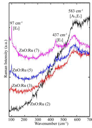
Figure 12: Micro-Raman spectra of deposited ZnO:Ru films. a) 2, b) 3, c) 5, and d) 7 immersions.L. Castañeda. et al.
Morphological Characterization
Atomic Force Microscopy Analysis
Figures. 3a-3d show the surface morphology, analyzed by AFM microscopy, of the ZnO:Ru thin films with different thickness. In the case of the samples deposited at two immersions the corresponding image Figure 13 (a) shows a porous structure composed of elongated grains separated by voids. In the case of films deposited from three immersions the AFM images Figure 13 (b) reveal a surface morphology composed by regular size grains and a few bigger grains. A close-up of these images confirms la agglomeration of secondary smaller grains. Additionally, it can be observed a separation among the grains by voids that are responsible for the porosity of the films. In this respect by an analysis of the micrographs with the WINSPM-Processing software of the microscope, we can easily distinguish the small secondary grains with a wide distribution grain size ranging from37 to 73 nm. The development of these stacked grains is a characteristic that is also consistent with the (002) preferential growth presented. In the AFM images Figure 13 (c-d), an intensity change of a virtual color in the x-y dimensional images is associated with depth in the z axis. In this way, the highest shining is associated with the top of the grains, whereas the full dark is associated with the bottom level. In addition, we can observe a lateral diameter of 30 nm and a thickness of 5 nm of the plates. Further studies are required in order to make clear this point. The surface profile or the rms roughness of the films was measured, and values between 5-11 nm were estimated.
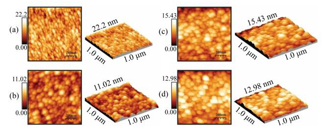
Figure 13: Bi-dimensional and three-dimensional AFM micrographs of ZnO:Ru thin films deposited from different immersions number. a) 2, b) 3, c) 5, and d) 7 immersions.L. Castañeda. et al.
Scanning Electron Microscopy
SEM analysis shows that the surface of the films is uniform and smooth. In fact, only for high magnifications it can be apparent the presence of round shaped small grains covering the substrate. Figures. 4a-d show the morphology of ZnO:Ru thin films with different film thickness. No significant difference in morphology of the films was encountered with film thickness variation, with the exception of Figure 13 (b) that shows grains with bigger size. Figure 15 presents theenergy dispersive spectroscopy (EDS) spectra revealing that the concentration of incorporated ruthenium [Ru] in the samples is much lower than the nominal concentration. Thus, the [Ru]/[Zn] atomic concentration ratio, varied from 0.02 to 0.07 at%; whereas the Zn:O proportion was stoichiometric, in the order of 1:1 for all the samples. Secondly, the incorporation of alkaline ions can be evidenced from the spectrum (Ca2+, Si4+, and Na+); these supposedly come from the substrate and were incorporated to the films during the growth process. Additionally, in order to prove the Ru incorporation to the ZnO lattice, as well as its concentration profile, SIMS analysis of the three immersions sample was carried out Figure 16. The profiles show that the Zn and O distribution is constant with the depth, nevertheless a slight Ru surface segregation can be observed. It is worth mentioning that other elements different from Ru, Zn and O were not quantified, then they are not being presented in the present profile. 3.5. Nonlinear optical properties
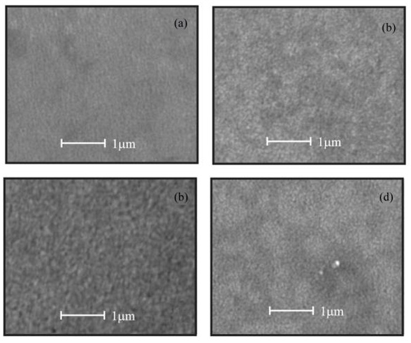
Figure 14: SEM micrographs of ZnO:Ru thin films deposited from different immersions number. a) 2, b) 3, c) 5, and d) 7 immersions.L. Castañeda. et al.
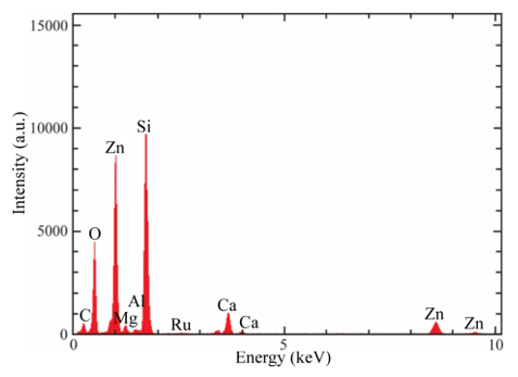
Figure 15: Typical EDS spectrum obtained in the three immersions ZnO:Ru sample.L. Castañeda. et al.
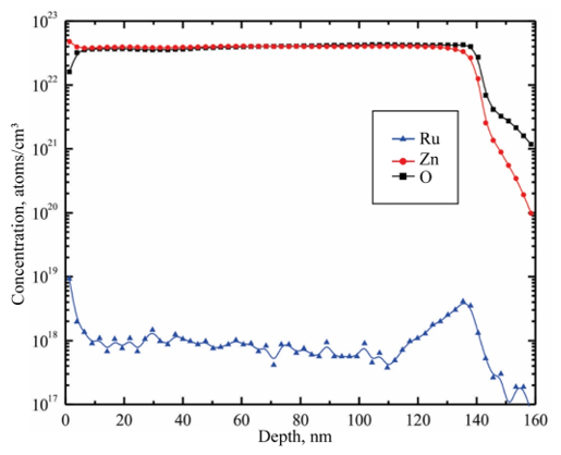
Figure 16: Typical SIMS analysis of the three immersions ZnO:Ru sample.L. Castañeda. et al.
The transmittance T as function of incident irradiance of three immersions ZnO:Ru sample is shown in Figure 17. This clearly describes a typical behavior of a strong two-photon absorption effect. The fit of the data was performed using the expression for the transmitted irradiance I(z) in the presence of nonlinear optical absorption:
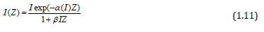
where b represents the two-photon absorption coefficient; I is the total irradiance of the incident beam, z is the thickness of the nonlinear optical media, and in our case the irradiance dependent absorption coefficient can be written asa ( 0 (I ) =α +β I ,with 0 α = 1.6 × 10⁶ m-1, and β = 1.8×10⁶ m/W, with an accuracy of 15 %. All deposited samplesshow a similar behavior. In order to improve the nonlinear optical properties-response of the ZnO:Ru samples further studies on the deposition conditions of the implemented sol-gel technique should be performed.
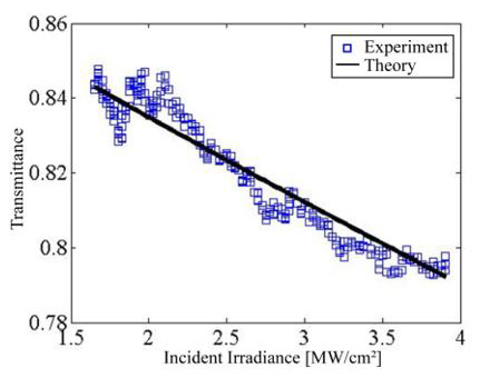
Figure 17: Optical transmittance vs incident irradiance for the three immersions ZnO:F sample.L. Castañeda. et al.
Sensing Properties
Figure 18 shows the performance of ZnO:Ru thin films as gas sensors when they are exposed at a controlled atmosphere of propane gas (C3H8) at different operating temperatures. In the case of the thinnest films (two immersions), an almost linear resistance change around two orders of magnitude was presented at the highest operating temperature (300 °C); however, at 100 and 200 °C no resistance changes were registered. As the film thickness increases, increasing resistance changes at 200 °C were observed. In addition, it is evident that the films measured at 300 °C show a shift in the reference resistance (C3H8 = 0 ppm), however it should not affect the gas sensitivity of the films. From the obtained results we can state that ZnO:Ru thin films with a thickness around 210 nm and operated at 300 °C in 500 ppm of C3H8 showed the highest resistance change, around two orders of magnitude, with a response time in the order of 60 s. On the other hand, the absence of a clear tendency of the sensing properties with the thickness can be associated with the non-intentional addition of other impurities coming from the substrate, as was proved by EDS analysis. According to our experience on processing of gas sensors thin films, this inconvenient effect is commonly presented in low-cost deposition techniques and by using sodocalcic glass substrates. In fact, the final annealing step in sol-gel synthesis causes exo-diffusion of alkaline elements, coming from the glass substrate, into the ZnO lattice that compensates “n-type” conductivity that necessarily affect the performance of the films in the gas sensing process as compared for similar films with no extra elements introduced into the lattice. However, based in the gas sensing results, it seems that, during the synthesis process, the hexagonal structure of ZnO causes that a fraction of alkaline elements are taking out from the ZnO lattice. Previous results of ZnO thin films, deposited by chemical techniques, based in Rutherford Backscattering Spectroscopy, shows that surface segregation of alkaline elements occurs. Despite these facts ZnO:Ru thin films deposited by sol-gel technique are still adequate for gas sensing applications.
Figure 18: Surface resistance variation as a function of C3H8 concentration at different operation temperatures for ZnO:Ru samples.L. Castañeda. et al.
Acknowledgments
The authors gratefully acknowledge the financial support from the EscuelaSuperior de Medicina, Instituto Politécnico Nacional, through Project no.20210385.
References
- P Kofstadt (1983) Nonstoichiometry, Diffusion and Electrical Conductivity in Binary Metal Oxides, R. E. Krieger, Malabar, FL, U.S.A, pp: 15-96-121.
- T Takeuchi (1988) Oxygen sensors. Sens. Actuators 14(2): 109-124.
- SA Akbar, LB Younkman (1997) J Electrochem. Soc 144(5): 1750.
- F A Cotton, G Wilkinson (1996) Basic Inorganic Chemistry, John Wiley & Sons, Inc. New York, U.S.A, pp: 441.
- RC Weast (Ed.) Handbook of Chemistry and Physics, 67th Edition, CRC Press, Boca Raton, FL, U.S.A, 1986–1987, pp.B-140.
- TY Tien, HL Stagler, EF Gibbons, PJ Zacmanidis (1975) Am. Ceram. Soc. Bull.54(1975): 280.
- L Castañeda, JC Alonso, A Ortiz, E Andrade, JM Saniger JG, et al. (2002) Spray pyrolysis deposition and characterization of titanium oxide thin films. Bañuelos Mater.Chem. Phys. 77(2002): 938-944.
- PK Dutta, A Ginwalla, B Hogg, BR Patton, B Chwieroth, et al. (1999) J. Phys. Chem. B 103(1999): 4412.
- Y Shimizu, N Kuwano, T Hyodo, M Egashira (2002) Sens. Actuators, B 83(2002): 195.
- CA Papadopoulos, JN Avaritsiotis (1995) A model for the gas sensing properties of tin oxide thin films with surface catalysts. Sens. Actuators, B 28(3): 105.
- A Mandelis, C Christofides (1993) Physics Chemistry and Techonology of Solid-State Gas Sensors Devices, John Wiley & Sons, Inc. New York, U. S.A pp. 122.
- N Yamazoe, J Fuchigami, JM Kishikawa, T Seiyama (1979) Interactions of tin oxide surface with O2, H2O and H, Surf. Sci. 86 (1979): 335-344.
- EL King (1964) How Chemical Reactions Occur, W.A. Benjamin, Inc., New York, USA, pp. 99.
- ML Bender, LJ Brubacher (1974) Catalysis and Enzyme Action, McGraw-Hill Book Company, New York, USA, pp. 89.
- Özgür Ü, AlivovYa I, Liu C, Teke A, Reshchikov MA, et al. (2005) A comprehensive review of ZnO materials and devices. J Appl Phys 98(4): 103.
- Janotti A, Van de Walle CG (2009) Fundamentals of zinc oxide as a semiconductor. Rep Prog Phys 72(12): 126501.
- Cooray NFY, Kushiya K, Fujimaki A, Okumura D, Sato M, et al. (1999) Optimization of Al-doped ZnO window layers for large-area Cu(InGa)Se2-based modules by RF/DC/DC multiple magnetron sputtering. Jpn J Appl Phys 38: 6213-6218.
- Segawa Y, Ohtomo A, Kawasaki M, Koinuma H, Tang ZK, et al. (1997) Growth of ZnO thin film by laser MBE: lasing of exciton at room temperature. Phys Status Solidi B 202(2): 669-672.
- Jayadev DN, Sainkar SR, Karekar RN, Aiyer RC (1998) Formulation and characterization of ZnO:Sb thick-film gas sensors. Thin Solid Films 325(1-2): 254-258.
- Yoshino Y, Makino T, Katayama Y, Hata T (2000) Optimization of zinc oxide thin film for surface acoustic wave filters by radio frequency sputtering. Vacuum 59(2-3): 538-545.
- Aly SA, El Sayed NZ, Kaid MA (2001) Effect of annealing on the optical properties of thermally evaporated ZnO films. Vacuum 61(1): 1-7.
- Kim HW, Kim NH (2004) Influence of the substrate on the structural properties of sputter-depositedZnO films. Phys Status Solidi A 201(2): 235-238.
- Katumba G, Olumekor L, Forbes A, Makiwa G, Mwakikunga B, et al. (2008) Optical, thermal and structural characteristics of carbon nanoparticles embedded in ZnO and NiO as selective solar absorbers. Sol Energy Mater Sol Cells 92(10): 1285-1292.
- Myoung JM, Yoon WH, Lee DH, Yun I, Bae SH, et al. (2002) Effects of thickness variation on properties of ZnO thin films grown by pulsed laser deposition. Jpn J Appl Phys 41(1): 28-31.
- Granqvist CG, Azensb A, Heszlerc P, Kishd LB, Osterlunde L, et al. (2007) Nanomaterials for benign indoor environments: Electrochromics for ‘‘smart windows’’, sensors for air quality, and photo-catalysts for air cleaning. Sol Energy Mater Sol Cells 91(4): 355-365.
- Bizarro M (2010) High photocatalytic activity of ZnO and ZnO:Al nanostructured films deposited by spray pyrolysis. Appl Catal, B 97(1): 198-203.
- Ko HJ, Yao T, Chen Y, Hong SK (2002) Investigation of ZnO epilayers grown under various Zn/O ratios by plasma-assisted molecular-beam epitaxy. J Appl Phys 92: 4354-4360.
- Minegishi K, Kikuchi Y, Yano K, Kasuga M, Shimizu A, et al. (1997) Growth of p-type zinc oxide films by chemical vapor deposition. Jpn J Appl Phys 36: L1453-1455.
- Znaidi L (2010) Sol–gel-deposited ZnO thin films: A review. Mater Sci Eng, B 174: 18-30.
- Katumba G, Mwakikunga BW, Mothibinyane TR (2008) FTIR and Raman spectroscopy of carbon nanoparticles in SiO2, ZnO and NiO matrices. Nanoscale Res Lett 3: 421-426.
- Bel Hadj Tahar R (2005) Structural and electrical properties of aluminum-doped zinc oxide films prepared by sol-gel process. J Eur Ceram Soc 25(14): 3301-3306.
- Mamat MH, Sahdan MZ, Khusaimi Z, Ahmed AZ, Abdullah S, et al. (2010) Influence of doping concentrations on the aluminum doped zinc oxide thin films properties for ultraviolet photoconductive sensor applications. Optical Materials 32(6): 696-699.
- Kim NJ, Choi SL, Lee HJ, Kim KJ (2009) Nanostructures and luminescence properties of porous ZnO thin films prepared by sol–gel process. Current Applied Physics 9(3): 643-646.
- Fathollahi V, MohammadpourAmini M (2001) Sol–gel preparation of highly oriented gallium-doped zinc oxide thin films. Mater Lett 50(4): 235-239.
- Silva RF, Zaniquelli MED (2004) Aluminium-doped zinc oxide films prepared by an inorganic sol-gel route. Thin Solid Films 449(1-2): 86-93.
- Epifani M (2007) Synthesis of nanocrystalline ZnO at low temperatures using inorganic sols as precursors. Mater Lett 61(14-15): 3100-3102.
- Srinivasan G, Gopalakrishnan N, Yu YS, Kesavamoorthy R, Kumar J, et al. (2008) Influence of post-deposition annealing on the structural and optical properties of ZnO thin films prepared by sol–gel and spin-coating method. Superlattices Microstruct 43(2): 112-119.
- Fujihara S, Sasaki C, Kimura T (2001) Effects of Li and Mg doping on microstructure and properties of sol-gel ZnO thin films. Journal of the European Ceramic Society 21(10-11): 2109-2112.
- Mridha S, Basak D (2007) Effect of thickness on the structural, electrical and optical properties of ZnO films. Mater Res Bull 42(5): 875-882.
- Ivanova T, Harizanova A, Koutzarova T, Vertruyen B (2010) Study of ZnO sol-gel films: effect of annealing. Mater Lett 64(10): 1147-1149.
- Zhou HM, Yi DQ, Yu ZM, Xiao LR, Li J, et al. (2007) Preparation of aluminum doped zinc oxide films and the study of their microstructure, electrical and optical properties. Thin Solid Films 515(17): 6909-6914.
- Paul GK, Sen SK (2002) Sol-gel preparation, characterization and studies on electrical and thermoelectrical properties of gallium doped zinc oxide films. Mater Lett 57(3): 742-746.
- Lee J-H, Park B-O (2003) Transparent conducting ZnO: Al, In and Sn thin films deposited by the sol–gel method. Thin Solid Films 426(1-2): 94-99.
- Girtan M, Socol M, Pattier B, Sylla M, Stanculescu A, et al. (2010) On the structural, morphological, optical and electrical properties of sol–gel deposited ZnO: In films. Thin Solid Films 519(2): 573-577.
- Yu Q, Yang H, Fu W, Chang L, Xu J, (2007) Transparent conducting ytrium-doped ZnO thin films deposited by sol-gel method. Thin Solid Films 515(7-8): 3840-3843.
- Musat V, Rego AM, Monteiro R, Fortunato E (2008) Microstructure and gas-sensing properties of sol–gel ZnO thin films. Thin Solid Films 516(7): 1512-1515.
- Sikhwivhilu LM, Mpelane S, Mwakikunga BW, Ray SS (2012) Photoluminescence and hydrogen gas-sensing properties of titanium dioxide nanostructures synthesized by hydrothermal treatments. Appl Mater Interfaces 4(3): 1656-1665.
- Ghimbeu CM, Schoonman J, Lumbreras M, Siadat M (2007) Electrostatic spray deposited zinc oxide films for gas sensor applications. Appl Surf Sci 253(18): 7483-7489.
- Öztas M, Bedir M (2008) Thickness dependence of structural, electrical and optical properties of sprayed ZnO: Cu films. Thin Solid Films 516(8): 1703-1709.
- Shinde VR, Gujar TP, Lokhande CD (2007) LPG sensing properties of ZnO films prepared by spray pyrolysis method: effect of molarity of precursor solution. Sens Actuators B 120(2): 551-559.
- Mitra P, Maiti HS (2004) A wet-chemical process to form palladium oxide sensitizer layer on thin film zinc oxide-based LPG sensor. SensActuators, B 97(1): 49-58.
- Aguilar-Leyva J, Maldonado A, Olvera ML (2007) Gas-sensing characteristics of undoped-SnO2 thin films and Ag/SnO2 and SnO2/Ag structures in a propane atmosphere. Mater Charact 58(8-9): 740-744.
- Barrett C, Massalski TB (1966) Structure of metals; crystallographic methods, principles, and data. New York, USA: McGraw-Hill. pp: 205.
- Warren BE (1990) X-Ray Diffraction. New York, USA: Dover. Pp. 253.
- Arguello CA, Rousseau DL, Porto SPS (1969) First-order Raman effect in wurtzite-type crystals. Phys Rev 181: 1351-1363.
