 Review Article
Abstract
Selected for HIVE Рroject Collaborations are Following: Intel Corporation (Santa Clara, California), Qualcomm Intelligent Solutions (San Diego, California), Pacific Northwest National Laboratory (Richland, Washington), Georgia Tech (Atlanta, Georgia), and Northrop Grumman (Falls Church, Virginia). “The HIVE program is an exemplary prototype to forge new R&D pathways that can deliver unprecedented levels of hardware specialization and to build the software infrastructure. The new software must not only be compatible with the new hardware, but also with the existing CPU and GPU. In addition, the new software must support a large amount of existing software used in the data science world. Part of the goal is to be able to connect existing software and libraries to the HIVE software framework to make it easier to use.
Keywords: Mass-Multithreaded Architecture; Hybrid Microprocessor; Data Flow Control; Graphical Representation of Programs; Specialized Accelerators; Massively Parallel Systems
Introduction
As described by DARPA, main HIVE goal is creation of a “graph analytics processor” which incorporates the power of graphical representations of relationships in a network more efficiently than traditional data formats and processing techniques according to DARPA. In combination with emerging machine learning and other artificial intelligence techniques that can categorize raw data elements. By updating the elements in the graph as new data becomes available, a powerful graph analytics processor could discern otherwise hidden causal relationships among the data elements in the graph representations [1]. DARPA suggests such a graph analytics processor might achieve a “thousand-fold improvement” in processing efficiency over today’s best processors, enabling the real-time identification of strategically important relationships as they unfold in the field rather than relying on after-the-fact analyses in data centers. Current software includes algorithms exposed via API, internal graph representation of data and hardware “backends” (GPU, CPU, ASIC). Chinese specialist Wang explained that under the current AI platforms major tradeoffs must be made, whether it is optimizing for a certain type of hardware or optimizing for certain algorithms. He said: “If you specialize in graph representation, then you will be disconnected from the data science ecosystem because you are “cut off” from some important libraries” [2]. As part of the second phase of HIVE, they are developing a modular architecture framework. Existing software is being reintegrated into their components so that they can be inserted into the framework according to the best features of the software.
The structure includes Workflow Scheduler and Dispatch Engine. They use the DASK task scheduler to perform scheduler and dispatch operations. In fact, they are fully targeted at a wide range of hardware so that data scientists can immediately span CPUs, GPUs and ASICs to take full advantage of the same software infrastructure. So, we can use PUMA graph processor to accelerate the load processes. Framework must include a set of converters that can convert data in different formats [2,3].
Basic Targets
In Russia we also promote proactive development of domestic
massively parallel processors. Objectives of the project also include
information and analytical work and the development of technical
solutions for creating high-speed element and design base. The basic
component of the processor is a tile formed by a 64-thread core,
connected by specialized accelerators (SFU). The massively parallel
processor must include connected by an on-chip network hundred
tiles, several links of an on-chip interaction, PCI-e interface with the
host processor. The ideology of massively parallel architecture is
similar to processor “Colossus” (company Graphcore) [4], focused
on machine learning tasks. But the domestic massively parallel
systems are hybrid and reconfigurable platforms. Now we will
look at the basic principles for the development of innovative AI
systems. DARPA project includes five key technologies:
a) Intelligent scheduling to manage the set of domain
resources in the context of specific applications. This should
be a technical focus of this project, and it is also the basis for
the realization of the project’s goals. Only by realizing runtime
intelligent scheduling can software and hardware be decoupled.
The performance of smart scheduling is directly related to the
efficiency of the final system. For the implementation of this part,
there are some further discussions in the technical description,
such as adding a processor dedicated to scheduling in the system,
allowing each PE to analyze and report its own running status.
b) Software tools to enable a development ecosystem that
exercises the full capability of the highly programmable system.
Software tools include development tools, such as compilers and
debuggers, algorithm libraries, applications and examples. Software
tools should be the most important part of whether specific
calculations can truly be implemented. A basic requirement is that
they can also support new designs in the field. DARPA strongly
encourages the use of existing software tools and also supports
Open-source work.
c) Forming domain representations as ontologies. This
is a job worthy of attention, how to describe a “Domain”. For
Domain-Specific software and hardware design work, the premise
of the design is a good description of the characteristics of this
field. However, these definitions are still too simple to reflect the
relationship between different groups.
d) Medium access control (MAC) to interconnect the PEs
and to allow the data throughput, taking into consideration latency,
power, and other domain constraints. In HIVE project the MAC
layer is the medium for exchanging data structures between PEs,
including physical structure, topology and a standard programming
interface.
e) Hardware integration of the right set of PEs on the MAC
layer with the operating scheduler and software into a fabricated
socket. The final result of this project also includes a heterogeneous
SoC hardware, but this does not seem to be the focus of this project.
According to the description of this project, PE is a concept with a
relatively large granularity, such as CPU, GPU, TPU, Neuromorphic
Unit, DSP and hardware accelerators.
Testing Results
In the field of dedicated processor and accelerator design
the performance competition is fierce. It has even become an
international-level scoring contest. Usually, international high-level
publications (such as ISSCC) publish the latest “scoring results”,
such as the performance comparison result of a CNN acceleration
chip shown in Figure 1 [5]. The scoring result does not represent
an absolute advantage, but it also becomes a measure of whether
the design can be recognized as a good design. But the benchmarks
obtained from the references are not completely comparable,
because each design has its own special features. In the article [6]
author hopes that readers can jump out of the thinking mode of
“mutual scoring” and get the best design possible in theory (from
the point of view of extreme design).
Analysis is traditionally divided into four parts:
a) Performance indicators of digital logic chips.
b) Checks and balances between indicators and trade-off
methods.
c) Limit quantitative design method.
d) Investigation and analysis of the reasons for not reaching
the optimal performance.
When we analyze chip architecture, we mainly need to consider
the following indicators, as shown in Figure 2 [4]:
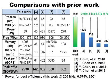
Figure 1: A “ scoring “ report announced at the ISSCC2017 meeting.
Figure 2: Collection of digital circuit performance indicators.
Single Standard (Orange Part)
a) Power consumption: static power consumption, dynamic
power consumption.
b) Energy consumption: the energy for processing a task.
c) Throughput: such as communication speed (bps), images
per second.
d) Delay: the time difference between input and output. For
real-time systems, latency is very critical.
e) Effective computing capacity: when performing a certain
calculation, the total number of operations per second is
calculated.
f) Peak computing capacity: the sum of computing
operations per second in the chip structure.
g) Clock frequency: adjustable clock frequency/voltage,
peak clock frequency.
h) Quantization accuracy: the data quantization width of
input/output/intermediate levels.
Normalization Standard (Purple Part)
Due to the checks and balances between indicators, an increase in an expected indicator may lead to an increase in other undesired indicators, so it needs to be measured by a normalized scale. This is often related to the application of the chip, such as: computing power normalized to power consumption; throughput normalized to energy; computing power normalized to the clock frequency and etc.
Comprehensive Results (Light Blue Part)
In the preliminary evaluation or sub-assessment, some comprehensive key indicators given by the comprehensive tool. These indicators are based on netlists and therefore do not include connections and can only be used for initial chip cost evaluation. Including: combinatorial logic resource cost, non-combination logic resource cost; device cost (such as RAM), combinatorial logic cost can also be measured by the number of equivalent gates. The difference is that the combinatorial logic overhead is related to the process library, while the number of equivalent gates is independent of the process library.
Memory Related (Dark Blue Part)
Memory is often represented as a black box. The number of memory chips, the capacity, depth and width of each memory chip. Whether it is dual-port or single-port (the size of dual-port is about twice as large as single-port). For small-scale memory less than 1KB or memory with many read and write ports, it is often implemented by register file size. When a smaller memory is needed or a storage device with a complex read-write interface is required, the register array is generally used to build it directly. The difference between the realization of the register array and the register file is that the register file often needs to be realized by a dedicated compiler, while the register array is directly realized by the hardware description language. The area of the register file will be much smaller than the equivalent function of the register array.
Interface and Bus Related (Grey Part)
Including the process library used, the number of wiring layers, operating voltage, low power consumption or high-performance process and etc.
Design Cost and Special Features (Pink Part)
a) For engineering research and development, it is also
necessary to consider the software/application development
cost and the ability to map new algorithms and parameters:
Time to market (TTM), non-refundable engineering expenses
(NRE) and etc.
b) Some chips tend to have advantages in other areas, such
as: boot time optimization, non-volatile, no fan requirements
(less than 4W), dynamic voltage frequency adjustment, gated
clock and other functions.
Conclusion
Similarly, integrating a new user API only needs to add an interface to one of the hardware and use at least one algorithm. Ultimately, the overall goal of HIVE is to unify and simplify the process of “optimizing the communication between graph software and hardware”. Reconfigurable hardware often needs to support multiple operating modes or operating parameters. Configurability and programmability are ultimately the need to add some redundancy to the original dedicated circuit to improve flexibility. But the efficiency of “ordinary” processors is not consistent. With proper ASIC design we can demonstrate good indicators for a limited class of “hard” logic algorithms. For a successful “breakthrough in the field of microelectronics” it is necessary to start developing a mass-parallel processor based on of multithread cores with specialized accelerators.
References
- https://www.fbo.gov/index?s=opportunity&mode=form&id=daa4d6dbee8741f56d837c404eac726d&tab=core&_cview=1
- Joel Emer, Vivienne Sze, Yu-Hsin Chen, Tien-Ju Yang (2021) Tutorial on Hardware Architectures for Deep Neural Networks.
- Benchmarking DNN Processors.
- Williams Samuel, Waterman Andrew, Patterson David (2009) Roofline: An Insightful Visual Performance Model for Multicore Architectures. Commun ACM 52 (4): 65-76.
- Wu Zhenzhi. The chip design method in pursuit of extreme performance.
- Introducing the Colossus™ MK2 GC200 IPU.
