 Short Communication
Abstract
The paper deals with the influence of the geometric shape of a semiconductor nanoparticle on the sensitivity of an optical plasmon sensor built on its basis. An ellipsoidal Indium-Tin Oxide (ITO) nanoparticle is considered as an example. It is shown that the sensitivity of such a sensor is proportional to the semiaxis dimension of the ellipsoid along which the polarization of the incident radiation is directed.
Keywords: Semiconductor nanoparticles; Localized surface plasmon resonance (SPR); absorbtion cross section; optical plasmonic sensor
Introduction
At present, almost all areas of human activities involve the use of nanoparticles for solving various technical issues [1-6]. One of the most perspective nanoparticles applications is biosensors [7-10]. Noble metals are mostly used materials for nanoparticle production due to their low reactivity, biological compatibility [11], high stability and catalytic activity [12]. Nevertheless, noble metal nanostructures have some important disadvantages: high cost and much limited ability to change a density of the free charge carriers [13]. The latter makes almost impossible to tune surface plasmon resonance parameters. From this point, semiconductor nanoparticles are rather cheap and flexible solution of this problem due to the doping opportunity (concentration of free charge carriers can be altered in the wide ranges that corresponds to the plasmon resonance frequencies in the diapason from the terahertz to the visible part of light spectrum) [14]. As a matter of fact, semiconductor materials are widely used in the biosensors design. For example, CdS and PbS nanoparticles are used for biomolecules labeling [15], polyaniline semiconductor films is a rather perspective solution for potentiometric biosensor development [16]. One more intriguing application is proposed in the work [17] devoted to Escherichia coli detection with use of photoluminescence-based quantum semiconductor biosensor. Despite the variability of approaches and applications, consideration of semiconductor nanoparticles plasmonic properties in the context of biosensor development is far from the exhaustive. This is the point to which the present work is devoted.
The processes of absorption and scattering of electromagnetic radiation on semiconductor spherical nanoparticles were considered earlier [18,19]. Based on the results obtained, a model of an optical plasmon sensor based on semiconductor nanoparticles was proposed [20]. This work is a continuation of the aforementioned works and sets the task of generalizing the model of an optical plasmon sensor to semiconductor nanoparticles of ellipsoidal shape, since the previously proposed model [20] is only a special case for specific nanoparticles. An analysis of the literature showed that this issue had not been investigated earlier, and the model [20] showed the promising prospects of using semiconductor nanoparticles in sensors based on surface plasmon resonance.
Materials and Methods
We find the photoabsorption cross section using the optical theorem:
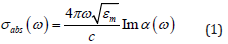
where ω is the frequency of laser radiation, εm is the dielectric permittivity of the medium in which the nanoparticle is placed, c is the speed of light in vacuum, α(ω) is the dynamic polarizability of the nanoparticle.
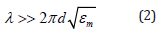
The calculation α(ω) is performed within the dipole approximation, i.e. for a nanoparticle, the maximum linear size d of which is significantly less than the wavelength λ of the incident radiation:
The geometry of a nanoparticle [21] is the ellipsoid. A rectangular coordinate system XYZ is introduced, the origin of which coincides with the geometric center of the ellipsoidal nanoparticle, and the axes OX, OY, OZ are directed along the semiaxes of the ellipsoid a, b, f respectively.
It is assumed that the electromagnetic wave is polarized along one of the i-th axis (i = X, Y, Z).
The expression for the polarizability along each of the axes is written as follows [21]:
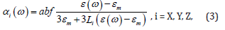
where ε(ω) – dielectric permittivity of a semiconductor nanoparticle.
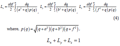
Geometric coefficients Li expressed as:
Dielectric permittivity of a semiconductor target ε(ω) for sufficiently low frequencies (in comparison with the band gap of the considered semiconductor) can be described by the classical Drude model [22,23]:
where ε∞ – high frequency dielectric permittivity, γ – relaxation constant, ωp – plasma frequency.
The Drude parameters (ε∞, ωp, γ) included in (5) can be found from the reference literature or determined from the absorption curves for the nanoparticles under consideration.
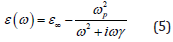
Below are the results of calculations of the photoabsorption cross section of ellipsoidal ITO nanoparticles [24]. ITO nanoparticles with Sn doping levels of 8 and 10 percent are considered, for which ωp=1.72 eV, γ = 0.22 eV and ωp=1.89 eV, γ = 0.15 eV correspondingly.
In both cases ε∞=4.08, dielectric permittivity εm = 1.
Let us choose the following values of the semiaxes of an ellipsoidal nanoparticle: а = 6 nm, b = 12 nm, f = 16 nm.
The curves in Figure 1 have the maxima that correspond to plasmon resonances. For both nanoparticles, the plasmon resonance amplitude increases with an increase in the length of the axis along which the radiation is polarized, and the plasmon resonance maximum shifts to a lower frequency region.
Figure 1: Dependence of the photoabsorption cross section for ITO nanoparticles with a doping level of 8% (red curves) and 10% (blue curves).
Discussion
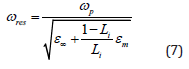
The position of the plasmon resonance maximum ωres can be found from the condition:
After performing mathematical transformations, we obtain the expression:
Expressing ωres in terms of the wavelength λres and taking into
account that  we obtain the expression:
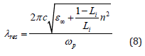
Let us construct dependences (8) of the wavelength of the maximum of the photoabsorption cross section λres on the geometric coefficient Li for ITO nanoparticles.
From Figure 2 it follows that the dependencies λres(Li) are monotonically decreasing with increasing Li, which corresponds to a decrease in the linear size of the nanoparticle along the i-th axis. At equal n, a larger shift of the maximum is observed for ITO nanoparticles with an 8% doping level. An increase in the refractive index n of the medium leads to an increase in the shift in the position of the maximum of the photoabsorption cross section for each type of nanoparticles at fixed Li. This effect underlies the principle of operation of optical plasmon sensors and allows one to determine the characteristics of the medium in which the nanoparticle is placed [20].
An important characteristic of such a sensor is the magnitude of the position shift λres when the refractive index of the medium surrounding the nanoparticles changes - the sensitivity parameter Sλ [19], which can be defined as follows:
\
Figure 2: Dependence of the position of the maximum of the photoabsorption cross section on the geometric factor Li for ITO nanoparticles with a doping level of 8% (red curves) and 10% (blue curves) at different refractive indices of the medium n.
Substituting (8) into (9), we obtain the expression for the sensitivity of an optical plasmon sensor on an ellipsoidal nanoparticle:
From expression (10) it is seen that the sensitivity Sλ, among others, is influenced by the value of the parameter Li. Let us investigate the influence of this parameter on the value Sλ. From Figure 3 it follows that a decrease in the parameter value Li leads to an increase in the sensitivity parameter Sλ, which corresponds to the stretching of a nanoparticle along the direction of radiation polarization, and the sensitivity of ITO nanoparticles with an 8% doping level, at the same Li, is higher than for an ITO nanoparticle with 10% - doping level. The dash-dotted curves in this graph correspond to the spherical case when Li = 1/3.
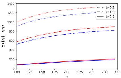
Figure 3: Dependence of the sensitivity parameter Sλ on the refractive index of the environment at various values of the parameter Li for ITO nanoparticles with a doping level of 8% (red curves) and 10% (blue curves), as in Figure 1 and Figure 2.
Conclusion
Within the framework of the dipole approximation, the photoabsorption cross section for ellipsoidal ITO semiconductor nanoparticles with a doping level of 8 and 10 percent was calculated. It is shown that the amplitude of the plasmon resonance increases with an increase in the size of the nanoparticle (the length of the semi-axis of the ellipsoid), along which the radiation is polarized, and the maximum of the plasmon resonance shifts to a lower frequency region. At equal refractive indices n, a larger shift of the plasmon resonance maximum is observed for ITO nanoparticles with an 8% doping level.
The calculation of the sensitivity of an optical plasmon sensor, which can be built on the basis of ellipsoidal nanoparticles, has been performed. It was found that stretching a nanoparticle along the direction of radiation polarization leads to an increase in the sensor sensitivity, and the sensitivity for ITO nanoparticles with an 8% doping level, at equal, is higher than for an ITO nanoparticle with a 10% doping level.
Acknowledgement
The reported study was funded by RFBR according to the research project № 19-07-00235 А.
References
- I Khan, K Saeed, I Khan (2019) Nanoparticles: Properties, applications and toxicities. Arabian journal of chemistry 12(7): 908-931.
- D L Fedlheim, C A Foss (2001) Metal nanoparticles: synthesis, characterization, and applications. CRC press.
- P Mohanpuria, N K Rana, S K Yadav (2008) Biosynthesis of nanoparticles: technological concepts and future applications. Journal of nanoparticle research 10(3): 507-517.
- A P Popov, A I Dimitrieva, A V Kovalenko, D S Yumanov, A V Stepanov et al. (2020) The structure of multi-walled carbon nanotubes as a factor affecting the life of E. Coli. Journal of Physics: Conference Series V 1611.
- Homola (2006) Surface plasmon resonance (SPR) sensors. In Surface plasmon resonance based sensors. Springer.
- S Gupta (2016) Exploration of Various Classes of Nanoparticles used in Cosmetic Applications. Int Res J of Science & Engineering 4(5): 91-97.
- Zhu Ningning, Zhu Chang, Pingang He, Yuzhi Fang (2005) Electrochemical DNA biosensors based on platinum nanoparticles combined carbon nanotubes. Analytica chimica acta 545(1): 21-26.
- Lazarides A A, K Lance Kelly, T R Jensen, G C Schatz (2000) Optical properties of metal nanoparticles and nanoparticle aggregates important in biosensors. Journal of Molecular Structure: THEOCHEM 529(1-3): 59-63.
- Saei Amir Ata, Jafar Ezzati Nazhad Dolatabadi, Parvaneh Najafi Marandi, Alireza Abhari, Miguelde la Guardia (2013) Electrochemical biosensors for glucose based on metal nanoparticles. TrAC Trends in Analytical Chemistry 42: 216-227.
- V V Ivanov, A A Efimov, D A Mylnikov, A A Lizunova (2018) Synthesis of Nanoparticles in a Pulsed-Periodic Gas Discharge and Their Potential Applications. Russian Journal of Physical Chemistry 92(3): 607-612.
- X Wang, C Xi (2018) Novel Nanomaterials for Biomedical, Environmental and Energy Applications. Elsevier.
- K S Siddiqi, A Husen (2016) Green synthesis, characterization and uses of palladium/platinum nanoparticles. Nanoscale research letters 11(1): 482.
- J A Faucheaux, A L D Stanton, P K Jain (2014) Plasmon Resonances of Semiconductor Nanocrystals: Physical Principles and New Opportunities. J Phys Chem Lett 5: 976-985.
- B H Nguyen, V H Nguyen (2015) Recent advances in research on plasmonic enhancement of photocatalysis. Adv Nat Sci Nanosci Nanotechnol 6(4).
- Luo Xiliang, Aoife Morrin, Anthony J Killard, Malcolm R Smyth (2006) Application of nanoparticles in electrochemical sensors and biosensors. Electroanalysis: An International Journal Devoted to Fundamental and Practical Aspects of Electroanalysis 18(4): 319-326.
- Karyakin, Arkady A, Lylia V Lukachova, Elena E Karyakina (1996) Potentiometric biosensors based on polyaniline semiconductor films. Sensors and Actuators B: Chemical 33(1-3): 34-38.
- Duplan Valérie, Eric Frost, Jan J Dubowski (2011) A photoluminescence-based quantum semiconductor biosensor for rapid in situ detection of Escherichia coli. Sensors and Actuators B: Chemical 160(1): 46-51.
- Bugaev A S, Astapenko V A, Manuilovich E S, Sakhno S V, Khramov E S, et al. (2018) Scattering of Electromagnetic Radiation by ITO Nanoparticles with Various Doping Levels, Doklady Physics 63(2): 55-57.
- Astapenko V A, Manuilovich E S, Sakhno S V, Khramov E S, Yakovets A V (2018) Absorption of Radiation by ITO Semiconductor Nanoparticles in Plasmon Resonance Region, Russian Journal of Physical Chemistry B 12(2): 325-329.
- Valeriy A Astapenko, Egor S Manuilovich, Sergei V Sakhno, Egor S Khramov, Evgeniya V Sakhno (2018) Optical plasmon sensor based on ITO nanoparticles Engineering and Telecommunication (EnT-MIPT) 978(1): 7281-0432.
- Bohren C F, Huffman D R (1983) Absorption and scattering of light by small particles. John Wiley & Sons 533.
- Kuttge M, Kurz H (2007) Analysis of the propagation of terahertz surface plasmon polaritons on semiconductor groove gratings. J Appl Phys 101(2).
- West P, Ishii S, V Naik, N K Emani, V M Shalaev et al. (2010) Searching for better plasmonic materials. Laser Photonics Rev 4(6): 795-808.
- Kanehara M, Koike H, Yoshinaga T, Teranishi T (2009) Indium Tin Oxide Nanoparticles with Compositionally Tunable Surface Plasmon Resonance Frequencies in the Near-IR Region J Amer Chem Soc 131: 17736.
