 Short Communication
Abstract
Integrated microfluidics has been well demonstrated as an irreplaceable advanced technology with abundant biomedical applications. Nevertheless, layout design of the microfluidic device can be challenging; and sometimes it can have limitations on connections among different microfluidic elements (e.g. pumps, chambers and mixers), especially for the highly integrated designs. Here, we present the design and fabrication of microfluidic via-holes, which offer fluidic connections between different microchannel layers. Analogous to the electrical via-holes in the printed circuit board design, these liquid via-holes can implement routing of the microchannels linking up different microfluidic elements within the same device. We implement the parallel mixing operation using a via-hole integrated microfluidic device. This work exhibits the application opportunities in the more general integrated bio-microfluidic devices.
Short Communication
High-throughput operation is one of the major objectives of microfluidics technology for biomedical applications [1]. Miniaturizing fluidic devices from microliters to picoliters in a multiplexed format has the potential to enable the parallel analysis of hundreds to thousands of biological samples while reducing reagent consumption. Microfluidic part fabrication based on soft lithography enables complicated and extremely compact device designs. In the fabrication process, the photolithography for mold fabrication and replica molding of polydimethylsiloxane (PDMS) using soft lithography is a standardized process for any arbitrary microfluidic channel network as a planar structure [2]. Building stacked layers through multilayer soft lithography principally relies on simple bonding of the molded layers, rather than the geometry of channel structures. Furthermore, the relative manufacturing efforts on a microfluidic chip line unit can be greatly reduced if a microfluidic chip is designed with a “unit” architecture, in which channel networks or valves can be operated in different configurations. Having flexible device architecture is particularly important for cell-based assays [3], which have relatively large undetermined variations and require multiple repeated experiments to statistically validate experimental hypotheses.
With a well-designed channel layout, many of the solution inlets/outlets and valve control ports can be shared among multiple device elements. Through design optimization, the number of required fluidic connections can be minimized, reducing off-chip work that includes solution preparation and connecting input (flow and control) lines into the devices. The risk of chip failure increases with the number of inputs, providing a strong motivation to put additional effort into channel routing and multiplexing strategies instead of making chips by a brute force, trial and error approach. However, routing of microchannel networks, particularly for high density co-planar designs [3], is non-trivial and limits the arrangements of microfluidic elements (e.g. pumps and mixers [4]) within the same device. Considering the analogy between the channels in microfluidic devices and wires in electronics, the concept of routing using electrical via-holes in printed circuit boards (PCBs) [5] is a traditional but still interesting strategy that can potentially solve some of the layout problems encountered in planar microfluidic networks. Electrical via-holes are placed between two layers of circuit patterns in electrical printed circuit boards. In this work, we adopt a similar strategy to establish a fabrication process compatible with the multilayer soft lithography to generate liquid via-holes between two flow layers of flow channels to provide fluidic connection in microfluidic devices.
Methods
Figure 1a illustrates the basic concept of applying microfluidic via-holes in device design. In case there exists a microchannel (A) blocking the connection between two flow lines (B1 and B2), a bridging flow channel (black), which connects to the two flow lines with via-holes (red), can be fabricated in another flow layer across the blocking channel. Therefore, flow line routing of the microchannel networks can be achieved by applying via-holes to connect the blocked flow lines with bridging channels. The implementation of via-holes into microfluidic devices enables higher-density layouts of microfluidic circuits, which is particularly appealing for high-throughput screening applications.
To fabricate the microfluidic via structures, a modified PDMS fabrication process was implemented for the double-layer flow structures connected with the microfluidic via-holes. Fabrication of the upper reflowed channel layer (channel height: 10μm) was achieved by conventional soft lithography, which is the replica molding of PDMS using patterned SU-8 epoxy (Microchem) on a silicon wafer as the mold. In this work, we added the separated lower layer using a special technique for multilayer interconnecting microfluidic channels. A mold for the lower flow layer was first prepared by patterning two SU-8 layers (with the 100μm tall via-holes (red rectangles in) (Figure 1b) on the 20μm thick fluidic channel structures (white layer in) (Figure 1b) on a 3-inch silicon wafer. Following mold salinization, a layer of 10:1 two-part PDMS (thickness: 150μm) was spin-coated on the mold. Two 5mm thick Poly-methyl methacrylate (PMMA) sheets and two transparency films (PP2500, 3M) were then placed above and below the mold in the configuration shown in Figure 1b. The stack of materials was then clamped and baked in an oven at 80°C for >10hr. After removing the PMMA sheets and transparency films, the SU-8/PDMS surface of the mold was aligned and bonded with the PDMS substrate with upper reflowed channel structures using an oxygen plasma machine. A razor blade was used to cutting along the device boundaries (red dotted lines in) (Figure 1b). Afterwards, the PDMS substrate containing via-holes was peeled off from the mold and bonded to the remaining part of the device to finish the fabrication process.
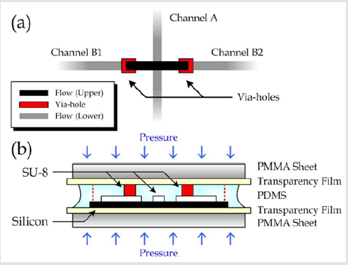
Figure 1:
a) Example of the bridging channel design.
b) Fabrication of microfluidic via-holes on a PDMS layer.
Results and Discussion
A microfluidic device including the via-hole structures was developed for the testing of a parallel mixing operation. The design was optimized as a parallel channel network, enabling the combination of a matrix of different solutions. The device layout (Figure 2a) contained an array of 4×4 chambers (diameter: 600μm), whose fluid flow was driven simultaneously by a shared peristaltic micropump [2]. Each chamber was connected to a “row” solution inlet and a “column” inlet, determined by its corresponding row (i)-column (j) index in the chamber array. The parallel mixing device (Figure 2b) consisted of control (thickness 20μm), upper (thickness: 10μm) and lower flow layers (100μm tall via-holes on 20μm thick microchannels), as indicated in the legend box in Figure 2. The two upper layers were fabricated by multilayer soft lithography, while the lower flow layer and fluidic via-holes were fabricated by the a fore mentioned method for two interconnecting layers of channel structures. Each of the 16 chambers connects to two solution channels (one from the top layer and one from the bottom layer) with a T-junction micromixer designed upstream the chamber for solution mixing [6]. Notably, the characteristic length of diffusion was half of the channel height (5μm) that the mixing can be achieved along T-junction microchannels indicated in Figure 2b.
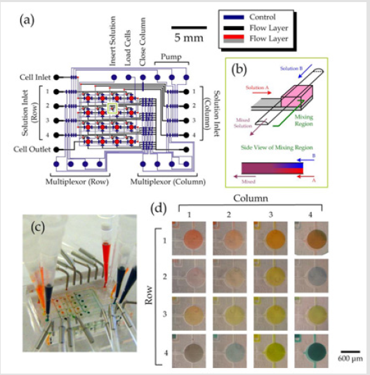
Figure 2:
a) Design layout of the parallel solution mixing operation.
b) Schematic of the mixer at the location highlighted in Fig. a.
c) Fabricated device.
d) The mixing performance was indicated by flow color dyes from the solution inlets..
As a demonstration, we applied color dyes to different solution inlets of the device in order to examine the parallel mixing operation (Figure 2c). The flow of dye solutions exhibited perfect fluidic connections across the via-holes. Because of the sequence of colors from solution inlets (red, transparent, yellow and blue for both row and column inlets 1 to 4, respectively), a chamber with row-column index (i, j) should have a similar color as another chamber with the skewed index (j, i). The color intensities of dye mixtures in the chambers (Figure 2d) exhibit success mixing of the inlet solutions with different ratios. It should be mentioned that the mixture ratio in each chamber was determined by the channel dimensions of the associated T-junction and the corresponding fluidic resistances. Overall, the work demonstrated the microfluidic via-hole designs can realize integrated microfluidic functions, such as parallel mixing. This microfluidic via-hole technique can be further applied to general microfluidic designs for biomedical and applications [7].
Acknowledgment
We acknowledge financial supports from General Research Grant (Project No. 11204317) of Hong Kong Research Grant Council.
Conflict of Interest
We declare that we do not have any economic/conflict of interest.
References
- G Du, Q Fang, JM den Toonder (2016) Microfluidics for cell-based high throughput screening platforms-A review, Analytica chimica acta 903: 36-50.
- MA Unger, HP Chou, T Thorsen, A Scherer, SR Quake (2000) Monolithic microfabricated valves and pumps by multilayer soft lithography, Science 288(5463): 113-116.
- P Cui, S Wang (2019) Application of microfluidic chip technology in pharmaceutical analysis: A review, Journal of Pharmaceutical Analysis 9(4): 238-247.
- CY Lee, CL Chang, YN Wang, LM Fu (2011) Microfluidic mixing: a review, International journal of molecular sciences 12(5): 3263-3287.
- R Venkateswaran, P Mazumder (1993) Coprocessor design for multilayer surface-mounted PCB routing, IEEE Transactions on Very Large Scale Integration (VLSI) Systems 1(1): 31-45.
- D Gobby, P Angeli, A Gavriilidis (2001) Mixing characteristics of T-type microfluidic mixers, Journal of Micromechanics and microengineering 11(2): 126.
- BK Gale, AR Jafek, CJ Lambert, BL Goenner, H Moghimifam, et al. (2018) A review of current methods in microfluidic device fabrication and future commercialization prospects, Inventions 3(3): 60.
