 Research Article
ABSTRACT
The present review paper reports on the physical properties, status, prospects for further development, applications of polycrystalline or amorphous, transparent and conducting oxides (TCO) semiconductors. The coexistence of electrical conductivity and optical transparency in these materials depends on the nature, number, and atomic arrangements of metal cations in crystalline or amorphous oxide structures, on the resident morphology, and on the presence of intrinsic or intentionally introduced defects. The important TCO semiconductors are impurity doped ZnO, In2O3, SnO2 and CdO, as well as the ternary compounds Zn2SnO4, ZnSnO3, Zn2In2O5, Zn3In2O6, In2SnO4, CdSnO3, and multi-component oxides consisting of combinations of ZnO, In2O3 and SnO2. Sn doped In2O3 (ITO) and F doped SnO2 TCO thin solid films are the preferable materials for most present applications. The expanding use of TCO materials, especially for the production of transparent electrodes for optoelectronic device applications, is endangered by the scarcity and high price of In.
This situation drives the search for alternative TCO materials to replace ITO. The electrical resistivity of the novel TCO materials should be ~10-5Wcm, typical absorption coefficient smaller than 104 cm-1 in the near UV and visible range, with optical band gap ~3 eV. At present, ZnO:Al and ZnO:Ga (AZO and GZO) semiconductors could become good alternatives to ITO for thin-film transparent electrode applications. The best candidates are AZO thin solid films, which have low resistivity of the order of 10−4 Wcm, inexpensive source materials, and are non-toxic. However, development of large area deposition techniques is still needed to enable the production of AZO and GZO films on large area substrates with a high deposition rate. In addition to the required electrical and optical characteristics, applied TCO materials should be stable in hostile environment containing acidic and alkali solutions, oxidizing and reducing atmospheres, and elevated temperature. Most of the TCO materials are n-type semiconductors, but p-type TCO materials are researched and developed. Such TCO include: ZnO:Mg, ZnO:N, IZO, NiO, NiO:Li, CuAlO2, Cu2SrO2, and CuGaO2 thin solid films. At present, these materials have not yet found place in actual applications.
Introduction
Most optically transparent and electrically conducting oxides (TCO) are binary or ternary compounds, containing one or two metallic elements. Their resistivity could be as low as 10-4 Wcm, and their extinction coefficient k in the optical visible range (VIS) could be lower than 0.0001, owing to their wide optical band gap (Eg) that could be greater than 3 eV. This remarkable combination of conductivity and transparency is usually impossible in intrinsic stoichiometric oxides; however, it is achieved by producing them with a non-stoichiometric composition or by introducing appropriate dopants. Badeker (1907) discovered that thin CdO films possess such characteristics [1]. Later, it was recognized that thin solid films of ZnO, SnO2, In2O3 and their alloys were also TCOs [2]. Doping these oxides resulted in improved electrical conductivity without degrading their optical transmission. Al doped ZnO (AZO), tin doped In2O3, (ITO) and antimony or fluorine doped SnO2 (ATO and FTO), are among the most utilized TCO thin solid films in modern technology. In particular, ITO is used extensively. The actual and potential applications of TCO thin solid films include:
(1) Transparent electrodes for flat panel displays
(2) Transparent electrodes for photovoltaic cells,
(3) Low emissivity windows,
(4) Window defrosters,
(5) Transparent thin solid films transistors,
(6) Light emitting diodes, and
(7) Semiconductor lasers.
As the usefulness of TCO thin solid films depends on both their optical and electrical properties, both parameters should be considered together with environmental stability, abrasion resistance, electron work function, and compatibility with substrate and other components of a given device, as appropriate for the application. The availability of the raw materials and the economics of the deposition method are also significant factors in choosing the most appropriate TCO material. The selection decision is generally made by maximizing the functioning of the TCO thin film by considering all relevant parameters and minimizing the expenses. TCO material selection only based on maximizing the conductivity and the transparency can be faulty.
Recently, the scarcity and high price of Indium needed for ITO, the most popular TCO, as spurred R&D aimed at finding a substitute. Its electrical resistivity (ρ) should be ~10-4Wcm or less, with an absorption coefficient (α) smaller than 104 cm-1 in the near- UV and VIS range, and with an optical band gap >3eV. A 100 nm thick film TCO film with these values for α and ρ will have optical transmission (T) 90% and a sheet resistance (RS) 10Ω At present, AZO and ZnO:Ga (GZO) semiconductors are promising alternatives to ITO for thin-film transparent electrode applications. The best candidates is AZO, which can have a low resistivity, e.g. on the order of 10−4 Wcm [3], and its source materials are inexpensive and nontoxic. However, the development of large area, high-rate deposition techniques is needed.
Another objective of the recent effort to develop novel TCO materials is to deposit p-type TCO films. Most of the TCO materials are n-type semiconductors, but p-type TCO materials are required for the development of solid lasers. Such p-type TCOs include: ZnO:Mg, ZnO:N, ZnO:In, NiO, NiO:Li, CuAlO2, Cu2SrO2, and CuGaO2 thin solid films. These materials have not yet found a place in actual applications. Published reviews on TCOs reported exhaustively on the deposition and diagnostic techniques, on film characteristics, and expected applications [4-6]. The present paper has three objectives:
(1) To review the theoretical and experimental efforts to explore novel TCO materials intended to improve the TCO performance,
(2) To explain the intrinsic physical limitations that affect the development of an alternative TCO with properties equivalent to those of ITO, and
(3) To review the practical and industrial applications of existing TCO thin solid films.
Electrical Conductivity
TCOs are wide band gap (Eg) semiconducting oxides, with conductivity σ in the range 102 – 1.2×10⁶ (S). The conductivity is due to doping either by oxygen vacancies or by extrinsic dopants. In the absence of doping, these oxides become very good insulators, with ρ > 1010 Ω-cm. Most of the TCOs are n-type semiconductors. The electrical conductivity of n-type TCO thin solid films depends on the electron density in the conduction band and on their mobility: σ=mne, where μ is the electron mobility, n is its density, and e is the electron charge. The mobility is given by:

where τ is the mean time between collisions, and m* is the effective electron mass. However, as n and τ are negatively correlated, the magnitude of μ is limited. Due to the large energy gap (Eg > 3 eV) separating the valence band from the conducting band, the conduction band cannot be thermally populated at room temperature (kT~0.03 eV, where k is Boltzmann’s constant), hence, stoichiometric crystalline TCOs are good insulators [7]. To explain the TCO characteristics, various population mechanisms and several models describing the electron mobility were proposed. Some characteristics of the mobility and the processes by which the conduction band is populated with electrons were shown to be interconnected by electronic structure studies [8] e.g., that the mobility is proportional to the magnitude of the band gap.
In the case of intrinsic materials, the density of conducting electrons has often been attributed to the presence of unintentionally introduced donor centers, usually identified as metallic interstitials or oxygen vacancies that produced shallow donor or impurity states located close to the conduction band. The excess or donor electrons are thermally ionized at room temperature and move into the host conduction band. However, experiments have been inconclusive as to which of the possible dopants was the predominant donor [9]. Extrinsic dopants have an important role in populating the conduction band, and some of them have been unintentionally introduce. Thus, it has been conjectured in the case of ZnO that interstitial hydrogen, in the H+ donor state, could be responsible for the presence of carrier electrons [10]. In the case of SnO2, the important role of interstitial Sn in populating the conducting band, in addition to that of oxygen vacancies, was conclusively supported by first-principle calculations of Kiliç and Zunger [11].
They showed that Sn interstitials and O vacancies, which dominated the defect structure of SnO2 due to the multivalence of Sn, explained the natural nonstoichiometry of this material and produced shallow donor levels, turning the material into an intrinsic n-type semiconductor [10]. The electrons released by these defects were not compensated because acceptor-like intrinsic defects consisting of Sn voids and O interstitials did not form spontaneously. Furthermore, the released electrons did not make direct optical transitions in the visible range due to the large gap between the Fermi level and the energy level of the first unoccupied states. Thus, SnO2 could have a carrier density with minor effects on its transparency [10]. The conductivity σ is intrinsically limited for two reasons. First, n and μ cannot be independently increased for practical TCOs with relatively high carrier concentrations. At high conducting electron density, carrier transport is limited primarily by ionized impurity scattering, i.e., the Coulomb interactions between electrons and the dopants.
Higher doping concentration reduces carrier mobility to a degree that the conductivity is not increased, and it decreases the optical transmission at the near-infrared edge. With increasing dopant concentration, the resistivity reaches a lower limit, and does not decrease beyond it, whereas the optical window becomes narrower. Bellingham et al. were the first to report that the mobility and hence the resistivity of transparent conductive oxides (ITO, SnO2, ZnO) are limited by ionized impurity scattering for carrier concentrations above 1020cm-3. Ellmer also showed that in ZnO films deposited by various methods, the resistivity and mobility were nearly independent of the deposition method and limited to about 2×10⁻⁴ Wcm and 50 cm2/Vs, respectively [12,13]. In ITO films, the maximum carrier concentration was about 1.5 ×1021 cm-3, and the same conductivity and mobility limits also held [14]. This phenomenon is a universal property of other semiconductors. Scattering by the ionized dopant atoms that are homogeneously distributed in the semiconductor is only one of the possible effects that reduces the mobility [15,16].
The all recently developed TCO materials, including doped and undoped binary, ternary, and quaternary compounds, also suffer from the same limitations. Only some exceptional samples had a resistivity of ≤1×10⁻⁴Wcm. In addition to the above-mentioned effects that limit the conductivity, high dopant concentration could lead to clustering of the dopant ions [17], which increases significantly the scattering rate, and it could also produce nonparabolicity of the conduction band, which has to be taken into account for degenerately doped semiconductors with filled conduction bands [18].
Optical Properties
As mentioned above, besides high conductivity (~106 S), effective TCO thin solid films should have a very low absorption coefficient in the near UV-VIS-NIR region. The transmission in the near UV is limited by Eg, as photons with energy larger than Eg are absorbed. A second transmission edge exists at the NIR region, mainly due to reflection at the plasma frequency. Ideally, a wide band gap TCO should not absorb photons in the transmission “window” in the UV-VIS-NIR region. However, there are no “ideal” TCOs thin solid films, and even if such films could be deposited, reflection and interference would also affect the transmission. Hence, 100% transparency over a wide region cannot be obtained.
The optical properties of TCOs transmission T, reflection R, and absorption A, are determined by its refraction index n, extinction coefficient k, band gap Eg, and geometry. Geometry includes film thickness, thickness uniformity, and film surface roughness. T, R and A are intrinsic, depending on the chemical composition and solid structure of the material, whereas the geometry is extrinsic. There is a negative correlation between the carrier density and the position of the IR absorption edge, but positive correlation between the carrier density and the UV absorption edge, as Eg increases at larger carrier density (Moss-Burstein effect). As a result, the TCO transmission boundaries and conductivity are interconnected.
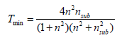
The width of the VIS transmission window of a TCO film with thickness deposited on a transparent substrate is affected not only by the optical parameters of the TCO film but also by the optical properties of the substrate. The refractive index nsub of the most common substrates are ~1.45 for fused silica and ~1.6 for various glasses. The extinction coefficient of the substrate (ksub) is generally < 10-7, hence any light absorption would take place in the film, where generally kfilm> ksub. For films thicker than 100 nm, several interference bands could be formed, producing maximal and minimal values of T when either the wavelength or thickness is varied. When kfilm ≈ 0, the peak transmission (Tmax) is equal to the transmission of the substrate [19]. Hence, assuming that the sample is in air, Tmax = 90% and 93% for films deposited on glass and fused silica, respectively. The minimum sample transmission (Tmin) in air is expressed by:
As most TCO films have values of n in the VIS in the range 1.8 – 2.8, Tmin will be in the range 0.8 – 0.52. Tmin is closely approximated by the relation: Tmin = 0.051n2-0.545n+1.654. As n in the VIS decreases with wavelength, Tmin increases with wavelength, but will not exceed ~0.8. When the film extinction coefficient is not negligible and affects the transmission, Tmax < Tsub, and Tmin also decreases. By decreasing the TCO film thickness, T is increased but the sheet resistance decreases. Combining together the optical and electrical properties of the film, the fraction of the flux absorbed in a film (A) is given by the expression:
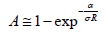
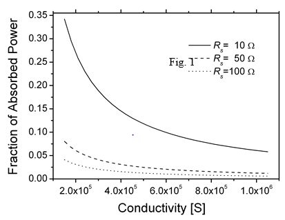
Figure 1: Fraction of absorbed power as function of TCO conductivity.
Figure 1 presents plots of the fraction of the absorbed power at wavelength of 400nm and k ~0.02 as a function of the conductivity for three representative values of RS. For a given σ, low values of RS necessitate using thick films, and lower conductivity requires the use of even thicker films, resulting in an increase in the loss of radiative power. The dependence of film thickness on the conductivity for three values of Rs is presented in Figure 2. Using the same film conductivity, applications requiring the lowest RS will be thicker and, and the absorbed fraction will be higher. At present, only high-quality ITO is compatible at present with the condition that the absorbed power fraction be lower than 10% and RS = 10Ω At lower extinction coefficient (k) films with lower conductivities can be used, e.g., when k = 0.002 instead of 0.02, the absorbed power A is lower by a factor of ~8 and allows the use of thicker films. The combination of film thickness, conductivity, and extinction coefficient determine the absorption of the radiation flux. However, when the total transmission T is considered, reflection and interference must be considered, which depend on the refractive indices of the substrate and the film, and the film thickness. A general formula for T and R was given by Cisneros [20].
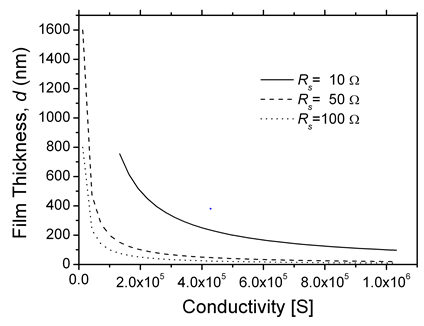
Figure 2: TCO film thickness as function of film conductivity.
Trends in the Development of TCO Materials
While the development of new TCO materials is mostly dictated by the requirements of specific applications, low resistivity and low optical absorption are always significant pre-requisites. There are basically two strategies in managing the task of developing advanced TCOs that could satisfy the requirements. The main strategy dopes known binary TCOs with other elements, which can increase the density of conducting electrons. As shown in Table 1, more than 20 different doped binary TCOs were produced and characterized [21], of which ITO was preferred, while AZO and GZO come close to it in their electrical and optical performance. Doping with low metallic ion concentration generates shallow donor levels, forming a carrier population at room temperature. Doping In2O3 with Sn to form ITO substantially increased conductivity. It is believed that substituting Sn4+ for In3+ provides carrier electrons, as Sn4+ is supposed to act as a one-electron donor [22]. Similarly, aluminum is often used for intentional n-type doping of ZnO, but other group III impurities, such as Ga and In, and group IV, such as Sn and Ge, also work.
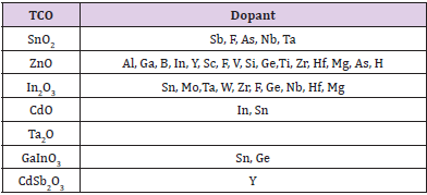
Table 1: TCO Compounds and Dopants.
Doping by Al produced the relatively high conductivity AZO.3 Doping with non-metallic elements is also common, e.g., ZnO:Ge (GZO), SnO2:F (FTO) and SnO2:Sb (ATO) [23,24]. Recently, AZO films with resistivity r~8.5.10-5 Wcm was reported by Agura, et al. [25]. An even lower resistivity was reported for GZO, ~8.1. 10-5 Wcm [26]. This ρ is very close to the lowest resistivity of ITO [27] of 7.7·10-5 Wcm, with a free carrier density of 2.5.1021 cm-3. The above-described metallic dopant ions should have appropriate valency to be an effective donor when replacing the native metallic ion. However, when an O2- ion is replaced with a F- ion, a donor level is again produced. Thus, doping SnO2 by F increased the carrier electron mobility by a factor of ~2 and their concentration also by a factor of 2, reducing the resistivity by a factor of 4 [28]. The concentration of F- dopant ions should not exceed an upper limit, as an increase in carrier scattering by F ions led to a decrease in the conductivity [29]. Doping SnO2 with Sb initially introduces Sb5+ ions that act as donors. When the doping concentration was increased beyond a certain level, however, Sb3+ ions began to replace the Sn4+ ions.
The introduction of Sb3+ ions generates an acceptor level that compensates the donors and increases the resistivity [30- 34]. This effort to increase the conductivity without degrading the transparency was paralleled by a more elaborate strategy in which phase-segregated two-binary and ternary TCOs were synthesized and characterized. The phase-segregated two-binary systems include ZnO-SnO2, CdO-SnO2, and ZnO-In2O3. In spite of the expectations, the electrical and optical properties of the twobinary TCOs were much inferior to those of ITO. The phase diagram of the ternary TCOs could be schematically presented by a threedimensional or four-dimensional phase combination of the most common ternary TCO materials [20,30] based on known binary TCO compounds. Accordingly, the ternary TCO compounds could be formed by combining ZnO, CdO, SnO2, InO1.5 and GaO1.5 to obtain Zn2SnO4, ZnSnO3, CdSnO4, ZnGa2O4, GaInO3, Zn2In2O5, Zn3In2O6, and Zn4In2O7. However, as Cd and its compounds are highly toxic, the utilization of these TCOs is limited, though they have adequate electrical and optical properties.
Other binary TCOs were synthesized from known binary TCOs and also from non-TCO compounds, such as In6WO12 and the p-type CuAlO2. The first-principle model of Kiliç and Zunger,10 showed the importance of the composition in turning an insulating oxide into a TCO. However, structural considerations should also be included. Hosono et al [31]. investigated the conditions for depositing widegap amorphous oxides with high electron mobility. They indicated that since the mobility is proportional to the width of the conduction bands, a large overlap between relevant orbitals is required. In addition, the magnitude of the overlap needs to be insensitive to the structural randomness that is intrinsic to the amorphous state. They assumed that since the spatial spreading of the ns orbital is large and the overlap between these ns orbitals with spherical symmetry is large and insensitive to any angular variations in the M-O-M bonds (where M is a metal cation) compared with p-p or d-p orbitals having high anisotropy in geometry.
Oxides composed of metal cations with an electronic configuration (n-l)d10ns0 would satisfy these requirements, as the lowest part of the conduction band in these oxides is primarily composed of ns orbitals [32]. Hosono et al. also conjectured that because of this, ternary oxides are preferred to binary oxides for the formation of amorphous TCO thin solid films. Scanning the periodic table, they identified 105 combinations of elements as promising ternary oxide candidates. As indicated by Mizoguchi and Woodward,7 not only do binary n-type TCO materials contain a metal with (n -1)d10ns0 electronic configuration, but also the ternary and quaternary complex TCOs. In a study of CdSnO3, Cd2SnO4, and CdIn2O4, Shannon et al. conjectured that the formation of a transparent conductor could result from edge sharing of Cd2+, In3+, and Sn4+ octahedra [33]. Nearly all of the complex TCOs found to date possess cations in octahedral coordination, as do most binary TCOs, with the exception of ZnO (wurtzite structure) and β-Ga2O3.
These and other studies show that similar complex oxides may be a rich source of new TCO materials [34-37]. Mizoguchi and Woodward concluded, however, that based on their research the only necessary condition for an oxide, binary or complex, to be a transparent conductor was to have a structure causing the lowest energy band to be dispersed and split off from the rest of the conduction band, whereas continuous edge sharing of the structural octahedra is only accidental [7]. The lowest energy band in the conduction band of an effective transparent conductor should be wide so that carriers introduced upon doping will be highly mobile. This condition is met when the anion coordination environment is fairly symmetric, as is the case in binary TCOs. This is a necessary but not sufficient condition for transparent conductivity. The second condition for a good TCO material is that it must be possible to effectively populate the conduction (or valence) band by doping, and that the doping should not seriously degrade the carrier mobility or the optical transmission [7,22].
Considering the ternary TCO compound (AxMyOz), where A is a lower valency cation and M is a main group ion with higher valency, if the valance of the A-O and M-O interactions were not too different, as they would be when the A-cation has an (n-1)d10ns0 electron configuration, the oxygen bonding was likely to remain reasonably symmetric and a disperse conduction band would result, in agreement with the necessary condition specified above. The dispersion of the conduction band energy in such compounds may not be as large as in a binary oxide, yet there could be extra freedom to manipulate the composition and structure of such oxides, facilitating the adaptation of the electronic energy levels for applications with specific needs [7]. All of the TCOs discussed above are n-type semiconductors. In addition, p-type doped TCOs were also developed and could find interesting future applications, in particular in the new optoelectronic field of “transparent electronics” [38]. Fabricating undoped or doped p-type TCOs was found to be more difficult than the n-type.
The first p-type TCO was made from CuAlO2 by Kawazoe in 1997 [39]. Prior to this, however, in 1993 Sato et al. reported on a semi-transparent p-type TCO with ~40% visible transmission [40]. It has been reported that is possible to form acceptor levels in ZnO, doping with N, P and As. The difficulty in producing p-type oxide was hypothesized to result from the strong localization of holes at oxygen 2p levels or due to the ionicity of the metallic atoms. O 2p levels are far lower lying than the valence orbit of metallic atoms, leading to the formation of a deep acceptor level with the holes. Hence, these holes are localized and require sufficiently high energy to overcome a large barrier height in order to migrate within the crystal lattice, resulting in poor hole-mobility and conductivity [41,42]. Following this hypothesis, an effort was made to grow p-type TCO based on “Chemical Modulation of the Valence Band (CMVB)”, where the oxide composition and structure were expected to delocalize the holes in the valence band.
The recent detailed report of Benerjee and Chattopadhyay [35] lists several groups of such synthesized p-type TCOs, e.g., CuMiiiO2, AgMiiiO2 where Miii is a trivalent ion. Compared with the n-type TCOs, these TCO have relatively lower conductivities, of the order of 1 S/cm, and lower transmission, < 80%. Growing p-ZnO was an important milestone in ‘‘Transparent Electronics’’, allowing fabrication of wide band gap p-n homo-junctions, which is a key structure in this field. It was anticipated that higher conductivity and optical transmission could be obtained by doping ZnO with N, F, P, Sb, and As, however, it was also shown that such doping had some serious limitations [43,44]. Based on first principle calculations, Yamamoto and Yoshida [45] proposed that co-doping of donoracceptor dopants (e.g. Ga and N, respectively) in ZnO might lead to p-type ZnO. Joseph et al. applied this principle to simultaneously dope ZnO with an acceptor (N) and a donor (Ga), where the acceptor concentration was twice that of the donor.
The optical transmission was greater than 85%, but the conductivity was low, ~1 S/cm [46]. p-type ZnO:Sb was deposited with a filtered vacuum arc equipped with a Zn cathode doped by Sb [47]. The conductivity was ~0.5 S/cm, the mobility 9-20cm2/ Vs and the hole density ~4·1016 cm-3, with transmission of ~85%. It is evident that the challenge to grow p-type TCO with ρ ~ 10-3 Ω.cm, or better, still exists. The need to produce n-type TCOs with higher conductivity and better transmission, without relying on In, inspired research and development effort to discover and study some unconventional TCOs. Novel transparent conductors were proposed using oxides with s2 electron configurations. Oxides of Mg, Ca, Sc and Al also exhibited the desired optical and electronic features; however, they have not been considered as candidates for achieving good electrical conductivity because of the challenge of efficiently generating carriers in these wide band gap materials. The approach suggested was to increase the mobility rather than the carrier density.
If this goal could be achieved, the optical properties would not deteriorate at lower resistivity. Recently, mobility with more than twice that of commercial ITO was observed in Mo-doped In2O3 (IMO), and it was shown that the conductivity can be significantly increased with no changes in the spectral transmittance upon doping with Mo [48,49], Electronic band structure investigations of IMO by Medvedeva revealed that the magnetic interactions which had never been considered to play a role in combining optical transparency with electrical conductivity ensure both high carrier mobility and low optical absorption in the visible range [50]. Recently, new thin film geometries were also explored in search of TCO films with higher conductivity. Dingle, et al [51]. showed that higher conductivity could be obtained by doping modulation, which spatially separates the conduction electrons and their parent impurity atoms (ions) and thereby reduced the effect of ionized and impurity scattering on the electron motion.
Rauf [52] used a zone confining process to deposit ITO with ρ = 4.4·10-5 Ω.cm and μ= 103 cm2/Vs. The highly and lowly doped regions were laterally arranged in the films, rather than vertically as in superlattice structures. A theoretical outline of a method to engineer high mobility TCOs was presented by Robbins and Wolden [53], based on the high mobility transistor structure discovered accidentally by Tuttle, et al. [54]. The film should consist of alternating thin layers of two semiconductors. One layer provides a high density of carriers, while the second is a high mobility material. Electrons are supplied by the former and transported in the latter, mitigating the limitations of ionized impurity scattering [50]. The model of Robbins and Wolden assumes that the electrons move into the high mobility material in response to differences in electron affinity.50 However, the success of the proposed TCO design depends upon controlling the layer thickness at nano dimensions, (e.g. ~5 nm).
In addition, this approach depends on having materials of excellent quality and compatible crystal structure in order to avoid problems related to interface defects. TCO materials with magnetic properties, which are ferromagnetic semiconductors with a Curie temperature well above room temperature, have also been explored recently, as they could be used for second generation spin electronics and as transparent ferromagnets. reported that Co doped ZnO thin film (Zn1-xCoxO) with x = 0.05 – 0.25, had a large magnetic moment of 1.8μB per Co ion for x = 0.05. High-temperature ferromagnetism was subsequently found by other groups, with varying magnetic moments.
Industrial Application of TCOs
TCO’s have diverse industrial applications – some of the more important ones will be described in this section. TCO coatings are applied to transparent materials used for work surfaces and closet doors, particularly in clean rooms used for electronics assembly, in order to prevent harmful static charge buildup. In this application relatively high surface resistances (e.g. kΩ/) can be tolerated. Transparent heating elements may be constructed from TCO coatings. These are applied as defrosters in aircraft and vehicular windshields. Their advantage over traditional hot air blowers is that they can have a much shorter effective defrosting time, and work uniformly over large areas. This application requires either the use of very low surface resistance coatings (e.g. ~1 Ω/)), or a high voltage power source. The application of TCO coatings to passenger vehicles has proven to be technically successful but a commercial failure, due to the high cost of a supplemental alternator to deliver the requisite high voltage. If the automobile industry will adopt a higher bus voltage, as has been widely discussed, then this application may prove to be more commercially feasible in the future.
TCO coatings may be used as shielding to decrease electromagnetic radiation interference (EMI) from providing visual access. This may be to either to keep radiation from escaping an enclosure, to avoid interfering with nearby devices, or detection, or from entering an enclosure to prevent external radiation sources from interfering with electronic devices within. One potential example is the window of domestic microwave ovens, which today use a perforated metal screen, which obscures clear visual observation, to reduce microwave leakage. Radiation leakage must be minimized to prevent harm to the users, as well as interference to proliferating wireless devices which use the unlicensed spectral band at 2.45 GHz. While transparent conducting films were proposed 50 years ago, an attempt to introduce microwave windows with TCO coatings into the market was not successful about a decade ago, due to the high cost. Low-cost designs are currently being developed.
The three largest applications of transparent conductive oxide thin solid films, in terms of the surface area covered, and their total value, are flat panel displays, solar cells, and coatings on architectural glass. In general, transparent electrodes are needed for a large variety of electro-optical devices, of which flat panel displays and solar cells are the most important examples. In liquid crystal displays (LCDs), TCO films are needed for both electrodes, in order to allow backlighting to pass through the liquid crystal film while applying voltage to the various pixels. Generally, these electrodes are in the form of a pattern of lines, with the alignment of the lines on the two electrodes perpendicular to each other. This allows addressing individual pixels by applying a voltage to the two lines which intersect at a given pixel. Thus, patterning the films is required. ITO is the TCO of choice in this application, both because of its electro-optical properties, and the relative ease of acid etching.
The best LCDs utilize an active matrix comprising one amorphous silicon transistor which occupies a corner of each pixel, and because the silicon is opaque, has reduced light transmission. Recently transparent field effect transistors (FETs) have been developed based on the zinc oxide but using a Cr gate. These zinc oxide FETs have been incorporated into small 220X280 10μm pixel active-matrix LCDs. Small and medium LCDs are a 25 B$/yr market which is growing by about 5%/yr, while large area LCDs have a similar market size and a much higher growth. The explosive growth for demand of ITO coatings for this specific application has generated widespread concern about Indium scarcity in the near future. Most solar cells use TCO films as a transparent electrode. Major considerations in the choice of the TCO for this application, besides the conductivity and transparency, are electronic compatibility with adjacent layers in the cell, processing requirements, and stability under environmental conditions.
Often tin oxide-based films are chosen for this application, in as much as patterning is not required, but environmental stability is. TCO films are commonly applied to architectural glass, often as part of multi-layer stacks. In window glass applications, usually the conductivity per se is irrelevant, but rather the concurrent high infra-red reflectivity is exploited, in order to obtain good light transmission in the visible range, while minimizing heat transmission. This feature is used to minimize air conditioning costs in the summer, and heating costs in the winter, in buildings equipped with appropriately coated windows. Approximately 25% of flat glass is coated, and energy conserving coatings are now mandated in various regions. Most commonly the coatings are applied by two techniques.
(1) Very enduring and inexpensive, but simple, coatings are produced with atmospheric pressure chemical vapor deposition (APCVD), in line with the float glass production process. This insures a fresh surface and exploits the high temperature of the glass during its production. However, APCVD is not very flexible and there are only limited options available for the coating architecture.
(2) A more flexible, but also more costly, process is magnetron sputtering. Commonly multiple (e.g. 20-60) rotary targets are mounted in long modular vacuum systems (e.g. 40-160 m length), and multilayer stacks are deposited as the glass panels pass beneath the various cathodes, traveling at velocities of ~1 m/s. Typically these systems operate continuously for 2 weeks, after which expended targets are replaced and other maintenance is performed.
Commercial Availability of TCO Thin Solid Films
The coating industry is segmented into “captive shops” which provide coating service within a given company for their products, and “job shops” which provide contract coating services for external companies. It is difficult to gather information about the former, since companies have no need to advertise their captive shops, and often prefer to guard their processes as trade secrets. More information is available concerning TCO availability from job shops, who often advertise their capabilities via the internet. A survey of these companies revealed that about ¾ of them indicated that they provide ITO coatings; most of the remainder did not specify the coating composition, but most probably they also deposit ITO as their TCO of choice. Only one company advertised supplying FTO films, and another also advertised IZO and AZO. Surface resistances ranged from 5 to 500Ω/. It should also be noted that float glass online coated by APCVD with FTO is readily available as an inexpensive commodity.
Conclusion
The expanding use of TCO materials, especially for the production of transparent electrodes for optoelectronic device applications, has developed into a worldwide multi-billion $US economy that in general depends on the availability of ITO. This economy is endangered by the scarcity and high price of In. The situation drives the search for alternative TCO materials to replace ITO and motivates an intensive investigation of the physics and chemistry of TCO materials. The main significant progress in the research and development of TCO thin solid films has been made in understanding the physics of TCO semiconductors. The physical processes that make possible the coexistence of electrical conductivity and optical transparency are well clarified and understood. In particular, the role of oxygen vacancies and various dopants in the formation of shallow donor levels is well established. In addition to binary TCOs, progress has also been made in developing new TCO compounds, consisting of combined segregated-binaries, ternary and quaternary oxides.
However, the objective of developing new TCOs with conductivity similar or even higher than that of ITO has not been realized. The conductivity of the recently developed ternary, quaternary, and binary-combination TCOs is lower than that of ITO. It is now appreciated that the attainment of higher conductivity is limited by the negative correlation between carrier density and electron mobility. It is now realized that the development of TCOs with higher conductivity does not necessarily depend on higher dopant concentration that provides higher carrier density but could also be achieved by maintaining moderate carrier density with increased mobility. Spatial separation of the conduction electrons and their parent impurity atoms (ions) should significantly reduce carriers scattering and increase their mobility. Using this principle, the conductivity of ITO was successfully increased, however, it has not yet been applied to other TCOs. The effort to produce TCOs with higher mobility based on using the oxides with ns2 electron configuration, instead of the ns0 electron configurations found in typical TCOs, was only partially successful.
These wide band gap oxides exhibited the desired optical and electronic features; however, their conduction was low due to too low. p-type TCOs were obtained by doping ZnO with N, F, P, Sb, and As, however, it was also shown that such doping had some serious limitations, and the conductivity was lower than n-type ZnO. In summary, AZO, GZO and FTO are at present the only TCOs with electrical conductivity close to that of ITO, and with appropriate high optical transmission in the near-UV, VIS and NIR. The objective of producing TCO materials with optical and electrical characteristics equivalent to those of ITO has not yet been achieved.
Conflicts of Interest
The authors declare no conflict of interest.
Acknowledgement
The author gratefully acknowledges the financial support from Universidad Estatal del Valle de Ecatepec.
References
- Baedeker K (1907) Ann Phys (Leipzig) 22: 749.
- Haacke G (1977) Transparent Conducting Coatings. Ann Rev Mater Sci 7: 73-79.
- Hiramatsu M, Imaeda K, Horio N, Nawata N (1998) J Vac Sci Technol A 16: 669.
- Lewis BG, Paine DC (2000) Materials Research Society Bulletin 25: 22-27.
- Exarhos GJ, Zhou XD (2007) Present Status of the Development and Application of Transparent Conductors Oxide Thin Solid Films. Thin Solid Films 515: 7025-7075.
- Fortunato E, Ginley D, Hosono H, Paine DC (2007) Transparent Conducting Oxides for Photovoltaics. MRS BULLETIN 32: 242-247.
- Edwards PP, Porch A, Jones MO, Morgan DV (2004) Basic materials physics of transparent conducting oxides. Dalton Trans 19: 2995.
- Mizoguchi H, Woodward PM (2004) Chem Mater 16(25): 5233.
- Look DC (2005) In: Claflin, Unterrainer K (Eds.)., Progress in Compound Semiconductor Materials IV-Electronic and Optoelectronic Applications, Boston, U.S.A., 2004, Materials Research Society Symposium Proceedings 829: B8.6.1.
- Van de Walle CG (2000) Hydrogen as a Cause of Doping in Zinc Oxide. Phys Rev Lett 85: 1012.
- Kiliç C, Zunger A (2002) Origins of Coexistence of Conductivity and Transparency in SnO2 Phys Rev Lett 88: 095501.
- Ellmer K (2000) J Phys D Appl Phys 33: R17.
- Ellmer K (2001) Resistivity of polycrystalline zinc oxide films: current status and physical limit.
- Frank G, Köstlin H (1982) Appl Phys A 27: 197.
- Masetti G, Severi M, Solmi S (1983) Modeling of carrier mobility against carrier concentration in arsenic-, phosphorus-, and boron-doped silicon. IEEE Trans Electron Devices ED30: 764.
- Chattopadhyay D, Queisser HJ (1981) Electron scattering by ionized impurities in semiconductors. Rev Mod Phys 53: 745.
- Ebert P, Zhang Z, Kluge F, Simon M, Zhang Z (1999) Urban Phys Rev Lett 83: 757.
- Pisarkiewicz T, Zakrzewska K, Leja E (1989) Thin Solid Films 174: 217.
- Cisneros JI (1998) Optical characterization of dielectric and semiconductor thin films by use of transmission data. Applied Optics 37: 5262-5270.
- Minami T (2005) Transparent conducting oxide semiconductors for transparent electrodes Semicond. Sci Technol 20: S35.
- Bellingham JR, Phillips WA, Adkins CJ (1992) Electrical and optical properties of amorphous indium oxide. J Phys Matter 2: 6207.
- Minami T, Sato H, Nanto H, Takata S (1986) Highly Transparent and Conductive Zinc-Stannate Thin Films Prepared by RF Magnetron Sputtering. J Appl Phys Part 2: Lett 25: L776.
- Bae JW, Lee SW, Yeom GY (2007) Doped-Fluorine on Electrical and Optical Properties of Tin Oxide Films Grown by Ozone-Assisted Thermal CVDJ. Electrochem Soc 154: D34-D37.
- Agura H, Suzuki H, Matsushita T, Aoki T, Okuda M (2003) Low resistivity transparent conducting Al-doped ZnO films prepared by pulsed laser deposition. Thin Solid Films 445: 263.
- Park SM, Ikegami T, Ebihara K (2006) Effects of substrate temperature on the properties of Ga-doped ZnO by pulsed laser deposition. Thin Solid Films 513: 90-94.
- Ohta H, Orita M, Hirano M, Tanji H, Kawazoe H, et al. (2000) Highly electrically conductive indium–tin–oxide thin films epitaxially grown on yttria-stabilized zirconia (100) by pulsed-laser deposition. Appl Phys Lett 76: 2740.
- Shanthi E, Banerjee A, Dutta V, Chopra KL (1982) Electrical and optical properties of tin oxide films doped with F and (Sb+F). J Appl Phys 53: 1615.
- Thangaraju B (2002) Structural and electrical studies on highly conducting spray deposited fluorine and antimony doped SnO2 thin films from SnCl2 Thin Solid Films 402: 71-78.
- Kurz A, Brakecha K, Puetz J, Aegerter MA (2006) Strategies for novel transparent conducting sol–gel oxide coatings. Thin Solid Films 502: 212-218.
- Hosono H, Yasukawa M, Kawazoe H (1996) Novel oxide amorphous semiconductors: transparent conducting amorphous oxides. J Non-Cryst Solids 203: 334-344.
- Robertson J (1979) Electronic structure of SnO2, GeO2, PbO2, TeO2 and MgF2. J Phys C12: 4767.
- Shannon RD, Gilson JL, Bouchard RJ (1977) Single crystal synthesis and electrical properties of CdSnO3, Cd2SnO4, In2TeO6 and Cdln2O4. J Phys Chem Solids 38: 877-881.
- Kawazoe H, Ueda N, Un’no H, Omata T,Hosono H, et al. (1994) Generation of electron carriers in insulating thin film of MgIn2O4 spinel by Li+ J Appl Phys 76: 7935.
- Cava RJ, Phillips JM, Kwo J, Thomas GA, Van Dover RB, et al. (1994) Transparent conducting thin films of GaInO3. Appl Phys Lett 64: 2071.
- Minami T (2000) New n-Type Transparent Conducting Oxides. Mater Res Soc Bull 25: 38-44.
- Freeman AJ, Poeppelmeier KR, Mason TQ, Chang RP, Marks TJ (2000) J Mater Res Soc Bull 25: 45.
- Banerjee AN, Chattopadhyay KK (2005) Recent developments in the emerging field of crystalline p-type transparent conducting oxide thin films. Progress in Crystal Growth and Characterization of Materials 50: 52.
- Kawazoe H (1997) P-type electrical conduction in transparent thin films of CuAlO Nature 389: 939.
- Sato H, Minami T, Takata S, Yamada T (1993) Transparent conducting p-type NiO thin films prepared by magnetron sputtering. Thin Solid Films 236: 27-31.
- Kawazoe H, Yanagi H, Ueda K, Hosono H (2000) Transparent p-Type Conducting Oxides: Design and Fabrication of p-n Heterojunctions. MRS Bull 25: 28-36.
- Fraga S, Karwowski S, Saxena KMS (1976) Handbook of Atomic Data, Elsevier, Amsterdam.
- Pearton SJ, Norton DP, Ip K, Heo YW, Steiner T (2005) Recent Progress in Processing and Properties of ZnO. Progress in Materials Science. Progress in Materials Science 50: 293.
- Zhang SB, Wei SH, Zunger A (1998) A phenomenological model for systematization and prediction of doping limits in II–VI and I–III–VI2 compounds. J Appl Phys 83: 3192.
- Yamamoto T, Yoshida HK (1999) Solution Using a Codoping Method to Unipolarity for the Fabrication of p-Type ZnO. Jpn J Appl Phys 38: L166.
- Joseph M, Tabata H, Kawai T (1999) Production Considerations for Europium-152 Teletherapy Sources Including Design of a Source Capsule with Intrinsic Beam-Hardening Capability. Jpn J Appl Phys 38 L1505.
- David T, Goldsmith S, Boxman, "p-Type Sb-Doped ZnO Thin solid films Prepared with Filtered Vacuum Arc Deposition", Proceeding Society of Vacuum Coaters (SVC) 47th Annual Technical Conference, pp. 27-31. S
- Meng Y, Shen J, Jiang YM, Zhang ZJ, Hua ZY (2001) Thin Solid Film 394: 219.
- Yoshida Y, Wood DM, Gessert TA, CouttsB TJ (2004) Indium oxide a transparent, wide-band gap semiconductor for (opto)electronic applications. Appl Phys Lett 84: 2097.
- Medvedeva JE (2006) Phys Rev Lett 97: 086 401.
- Dingle R, Störmer HL, Gossard AC (1978) Electron mobilities in modulation‐doped semiconductor heterojunction superlattices. Appl Phys Lett 33: 665.
- Rauf I (1993) Mater Lett 18: 123
- Robins JJ, Wolden CA (2003) Appl Phys Lett 83: 3933.
- Tuttle G, Kroemer H (1989) J Appl Phys 65: 5239.
- Ueda K, Tabata H, Kawai T (2001) Appl Phys Lett 79: 988.
- Hirao T, Furuta M, Hiramtsu T (2008) “ZnO-based TFT for use in LCD” 35th Int. Conf on Metallurgical Coatings and Thin solid films, San Diego.
