info@biomedres.us
+1 (502) 904-2126
One Westbrook Corporate Center, Suite 300, Westchester, IL 60154, USA
Site Map

Received: October 24, 2017; Published: November 08, 2017
Corresponding author: Av Moholkar, Department of Basic Science and Humanities Gokul Shirgaon, KITS College of Engineering Kolhapur, India
DOI: 10.26717/BJSTR.2017.01.000504
The effect of precursor concentration on the physico-chemical properties of cadmium oxide (CdO] thin films deposited using simple and effective chemical spray pyrolysis technique (SPTJ is studied for the first time. The X-ray diffraction study shows polycrystalline, face centered cubic structure of CdO films. Field emission scanning electron micrographs and cross-sectional images of CdO thin films shows that morphology of films changes from rough to smooth and thickness of the films increases from 794 nm to 1523 nm, as cadmium content increased in spraying solution. X-ray photoelectron spectroscopy confirms presence of 4d, 4s, 3d5/2, 3d3/2, 3p3/2, 3p1/2 fine structural states of cadmium and 1s fine structure state of oxygen. The optical study shows that the direct band gap energy values decreases from 2.58 to 2.42 eV with increase in precursor concentration which is attributed to B-M effect. The Hall Effect measurement indicates that all the films exhibit n-type semiconducting behavior, the electrical resistivity decreases from 34.5 x 10⁻⁴ to 2.7 x 10⁻⁴ Ωcm for 0.025M to 0.1 M solution concentration and further increase to 12.5 x 10⁻⁴ Ωcm for 0.125 M concentration. The CdO thin film deposited with 0.1 M precursor concentration exhibits the best optoelectronics properties amongst the all other CdO films. It shows transmittance of 74 %, high figure of merit of 25.3 x 10⁻³ (Ω)-1, carrier concentration of 5.87 x 10²⁰ /cm3 and mobility of 40 cm2/Vs. Photoluminescence spectra of CdO thin film gives two significant photoemission peaks at 434 and 539.80 nm (green) when they are excited at 400 nm wavelengths
Keywords: Transparent conducting oxide; Spray Pyrolysis Technique; Carrier concentration; Figure of merit; Photoluminescence
Abbreviations: CdO: Cadmium Oxide; TCO: Transparent Conducting Oxide ; EDAX: Energy Dispersive X-Ray Analysis; FE-SEM: Emission Scanning Electron Microscopy; TC: Texture Coefficient
The first report of a transparent conducting oxide (TCOJ was published in 1907, when Badeker reported that thin films of Cd metal deposited in a glow discharge chamber could be oxidized to become transparent while remaining electrically conducting. Since then, the commercial value of these thin films has been recognized, and the list of potential TCO materials has expanded to include, for example, Al-doped ZnO, CdSnO2, SnO2, F-doped In2O3, and many others. TCOs are an essential part of technologies that require both large-area electrical contact and optical access in the visible portion of the light spectrum. High transparency, combined with useful electrical conductivity (>103 Scm-1), is achieved by selecting a wide-band gap oxide. Most of the useful oxide-based materials are n-type semiconductors that ideally have a wide band gap (>2.5 eV], the ability to be doped to degeneracy, and a conduction-band shape (dictating electron effective mass] that ensures that the plasma- absorption edge lies in the infrared range [1].
August 2000 issue of MRS Bulletin is well timed to provide an overview of TCO, included articles cover the industrial perspective, new n-type materials [2] by Tadatsugu Minami, new p-type materials [3] by Hiroshi Kawazoe, Hiroshi Yanagi, Kazushige Ueda, and Hideo Hosono, novel deposition methods, applications and processing of transparent conducting oxides [4] by Brian G. Lewis and David C. Paine, and approaches to developing both an improved basic understanding of the materials themselves as well as models capable of predicting performance limits. There is a renewed interest in research on TCOs, mainly due to its numerous different properties and applications.
Cadmium Oxide (CdOJ is one of the promising TCO having high absorption in the order of 103 cm-1, high transmittance > 75 % , band gap of ~2.3 eV and high conductivity in the order of 104 S/m, made it applicable in photodiodes [5], phototransistors [6], photovoltaic cell [7], transparent electrodes [8], liquid crystal displays [9], UV detectors and UV-emitting diodes [10]. The properties of a TCO layer depend not only on its chemical composition, but also on the method used for its preparation. These preparative methods include physical methods (sputtering, evaporation, pulsed laser deposition) and chemical methods (chemical vapor deposition, sol-gel, and chemical bath deposition, electro-plating). There are number of physical and chemical techniques of thin film deposition. Amongst these various deposition techniques, the spray pyrolysis technique (SPT) is one of the chemical techniques which have many advantages compared to other chemical or physical technique such as low cost, easy to handle, easy doping, vacuum does not required at any stage, comparably more adherent films are formed in single step deposition and various properties of films can be tuned by varying the preparative parameters of the SPT, like substrate temperature, quantity of spraying solution, concentration of precursor solution, nozzle to substrate distance, spray rate etc. [11].
In our previous work [12], it is found that CdO films deposited at 350oC substrate temperature and quantity of 40 ml precursor solution with thickness of 1371 nm shows the best results like low resistivity of 3.7 x 10⁻⁴ Ωcm, high carrier concentration of 7.3 x 10 20 cm'3, mobility of 23.11 cm2/Vs and figure of merit of 18.23 Ω-1. There are very few reports on effect of concentration on various properties of TCO materials. Baneto et al. [13] reported the effect of precursor concentration on structural, morphological and opto- electric properties of ZnO thin films prepared by spray pyrolysis where it is revealed that morphology significantly depends on the precursor concentration, which is governed by nucleation and/or growth process. It is also verified that the optoelectrical properties of the films can be tuned by depositing films with proper precursor concentration. Effect of concentration of SnCl4 on different phsico- chemical, optical, electrical sprayed fluorine doped tin oxide thin films have been studied by Moholkar et al. [14].
Effect of ageing of the precursor solution on the structural, morphological, optical and electrical properties of ternary Cd ZnO thin films was studied by Balu et al. [15] where they have found that the Cd ZnO film prepared from 3 days aged precursor solution exhibit better surface morphology and the optical band gap decreased with increase in aging period of the starting solution which is attributed to quantum confinement effect. In one more report, Helen et al. [16] studied the influence of precursor concentration on the properties of spray deposited CdO thin films. It is found that the transmittance gets enhanced with increase in precursor concentration whereas the optical energy band gap value decreases from 2.50 eV to 2.37eV. Electrical studies revealed that the CdO thin film prepared using 0.15 M solution possesses lowest resistivity in the order of 10-4 Ωcm. So far there are no reports on the properties of sprayed CdO thin films in which effect of precursor concentration is studied. In the present investigation, CdO thin films have been deposited on glass substrate with different concentration of cadmium precursor solution by SPT and their structural, morphological, compositional, optical and electrical properties have been studied.
CdO thin films were deposited by SPT as described in our previous report, using aqueous solution of cadmium acetate [(Cd (CH3COO)2] as a precursor with slight modifications [17]. The solution of 0.025 M to 0.125 M concentration Cd(CH3COO)2 [LobaChemie Pvt. Ltd. Mumbai, India] was prepared in double distilled water (DDW), and sprayed onto the preheated ultrasonically cleaned glass substrates at 350oC temperature and further allowed to cool at room temperature. The other parameters like quantity, substrate temperature, spray rate, nozzle to substrate distance were kept constant throughout this experiment. All the obtained films were appeared as faint yellowish in color, transparent, well adherent to the substrates and pinhole free. Such obtained films were further characterized by using various characterizing tools. The structural properties were studied by X-ray powder diffractometer [Bruker AXS, D2-Phaser, USA] using Cu Kα (λ. = 1.5406 Å) operated at 30 KV, 20 mA. The micro structural study was carried out using field emission scanning electron microscopy (FE-SEM) [Hitachi S - 4800, Japan]. The thickness of the thin films was obtained from the cross sectional FE-SEM images. Energy dispersive X-ray analysis (EDAX) connected with FE-SEM was carried for confirming elemental presence in deposited film. The fine structural states of cadmium and oxygen were obtained from XPS study [Kratos Analytical, ESCA 3400, UK] [18]. The transmission and optical absorption spectra were studied at room temperature within 400 - 800 nm wavelength range using UV-vis spectrophotometer [Shimadzu UV- 1800, Japan]. The room temperature electrical measurements were carried out with Hall Effect set up in van-der Pauw configuration [SES Instruments, Roorkee, India]. The photoluminescence spectra were recorded using spectrofluorometer [Fluromax - 4, Japan].
The XRD patterns of0.025 M, 0.05 M, 0.075 M, 0.1 M and 0.125 M CdO thin films deposited at 350oC substrate temperature is shown in (Figure 1). All CdO thin films prepared with different precursor concentrations shows good match with pure CdO film when compared with JCPDS card number 01-075-0592 [18]. Three major peaks corresponding to (111), (200) and (220) planes obtained in XRD pattern, represents the polycrystalline face centered cubic structure of the CdO thin films. Along with these peaks, two minor peaks corresponding to (311) and (222) planes are also observed. The crystallite size is estimated using the Scherrer’s formula [19].
Figure 1: XRD patterns of 0.025 M - 0.125 M CdO films deposited at 350 oC substrate Temperature.

The average crystallite size obtained for 0.025 M, 0.05 M, 0.075 M, 0.1 M and 0.125 M CdO thin films from XRD data are 18.72 nm, 33.60 nm, 25.17 nm, 35.75 nm and 26.50 nm respectively. This variation in crystallite size can be correlated to the increased cadmium content in film with increase in concentration as well as to the increased thickness [20]. Though the concentration increases the location of the diffraction peaks does not change significantly but the XRD intensity strongly varies with the concentrations of cadmium precursor solution. The initial increase in the XRD peaks for CdO thin film can be explained by the creation of new nucleation centers due to the Cd atoms.
The subsequent decrease in the XRD peak intensities for higher concentration can be described by two factors; firstly, by the saturation of the newer nucleation centers and secondly, due to the change of the energy absorption at the time of collision, and of the physical and chemical interaction between ad-atoms and the film. The decrease in crystallite size to 23.61 nm for 0.125 M CdO film is due to the saturation of cadmium in the film for higher concentration [21]. The crystallites in a polycrystalline material normally have a crystallographic orientation different from that of its neighbors. The preferred orientation of the films is described by texture coefficient (TC), which is evaluated from equation [22],

The calculated TC values are depicted in Table 1, from the measured TC values, it is clear that all films have preferential orientation along (111) and (200) planes as the TC values calculated for these planes are greater than one. It is observed that the peak intensity along (111) and (200) plane of the film enhances when concentration of solution is increased from 0.025 M - 0.1M and the peak intensity decreased for 0.125 M CdO film it may be due to saturation of cadmium at this high concentration in film.
Table 1: The values of 20, (hkl), TC, a, e, D and 8 for sprayed CdO thin films with different cadmium acetate concentration deposited at 350 0C.

The lattice constants obtained corresponding to different planes is ~4.68 Å and standard lattice constant of CdO is 4.69 Å, it means that the compressive strain is present in the deposited films. The strain in the CdO film is determined using the equation [23].
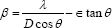
The average strain in the film is obtained by taking slope of a graph of (βcosθ)/λ Vs sinθ/λ. (Figure 2) shows such a graph of 0.1 M CdO thin film. It is seen in that all the points do not lie on a linear fitted straight line which represents that strain is present in the CdO film and it is 1.95 x 10⁻² in 0.1 M CdO thin film. The average strain evaluated for all other CdO films are depicted in Table 1, it varies nonlinearly between 1.66 x 10⁻² - 2.56 x 10⁻². The initial increase in the strain with increase in precursor concentration may be due to change in crystallite size which influences the grain boundaries (Figure 3).
Figure 2: Williamson- Hall (W-H) plot of 0.1 M CdO film, for strain broadening.

Figure 3: Typical NRF plot to determine lattice constant of 0.1 M CdO film deposited at 350 oC using spraying solution quantity of 40 ml.

The dislocation density (δ), defined as the length of dislocation lines per unit volume, which varies with crystallite size ‘D’, has been estimated using the equation [24].

The lesser values of 'δ' obtained 0.782 x 10¹⁵ lines /m2 for the 0.1 M CdO thin films indicate and confirms the degree of crystallization is higher for it the dislocation density of other CdO films depicted in (Table 1). The values Braggs angle (2θ), Miller indices (hkl), texture coefficient (TC), lattice constant (a), strain (εs), crystallite size (D) and dislocation density (δ) of all the deposited CdO thin films are presented in (Table 1)
Figure 4: (a-e) Surface and cross-sectional FE-SEM images of CdO thin films deposited for 0.025M - 0.125 M precursor concentrations at 350 oC substrate temperatures.

Figure 4 shows the surface and cross-sectional FE-SEM images of CdO thin films prepared using 0.025 M to 0.125 M concentration of spraying solution 40 ml deposited at 350 oC substrate temperature. It is observed that all the films are, dense and strongly adherent to the substrates. The film deposited at 350 oC and precursor concentration of 0.025 M shows random arrangement of irregular shaped grain like structure which may be due to insufficient concentration of precursor solution concentration. The grains are well connected with very few voids. The thickness of 0.025 M CdO film is 794 nm. The micrograph of 0.05 M CdO film shows improvement in grain size and growth of film, it may be with increase in precursor solution concentration more nucleation centers are available for film growth, dumbbell like structure is seen, the thickness of the film observed is 997 nm. It has proper and well managed arrangement of larger grains having relatively less voids. The film deposited with 0.075 M has thickness of 1005 nm and it is observed that the grains are get agglomerated to form somewhat like spherical clusters and few voids are also seen in this film. With the further increase in concentration the void free continuous smooth film surface is obtained for 0.1 M CdO film, and thickness increased to 1371 nm.
Finally the film deposited at 0.125 M shows very compact surface morphology, the film nature is very compact and densely packed , no voids are seen all the surface of the film it may be due to the cadmium content in solution increases and saturated over the surface. The thickness of the 0.125 M CdO film is 1523 nm. This type of nature can be further ascribed to better crystallinity, low disordering into film structure [25]. The film thickness is found to be increased with increase in concentration of spraying solution from 0.025 M to 0.125 M which may be due to increased growth rate due to availability of more nucleation sites, also as with increase in concentration of precursor solution cadmium content increases which promotes the coalesce process.
Figure 5 shows the EDAX spectra of typical 0.1 M CdO thin film deposited at 350 oC substrate temperatures. From EDAX spectra, the presence of Cd and O elements in deposited CdO film is confirmed and their atomic percentages are found to be 58.23 at.% and 41.77 at.% respectively, indicating that the CdO thin films are sub-stoichiometry which leads to the semiconducting behavior and increase in carrier concentration of the CdO films. The typical EDAX spectrum shows CdO film is oxygen deficient which is one of the reason for improved electrical conductivity of the films.
Figure 5: EDAX of typical 0.1 M CdO thin film deposited at 350 oC substrate temperature using spraying solution quantity of 40 ml.

The XPS measurements is carried out for identifying the elements and their stoichiometry in the film, survey scan spectra of CdO film and narrow scan spectra of Cd and O are recorded separately for quantitative analysis and to identify the oxidation states of the Cd and O. Survey and detailed scan XPS spectra for Cd 3d, O 1s of 0.1 M CdO thin film deposited at 350oC substrate temperature shown in (Figure 6) It shows various peaks belonging to Cd, O, C and Auger electron transitions. Along with it various satellite peaks corresponding to other elements are also observed.
Figure 6: X-ray photoelectron spectroscopy (XPS) (a) survey scans of 0.1 M CdO thin film (b) Narrow scan XPS spectrum of 3d core level of cadmium in 0.1 M CdO thin film (c) Narrow scan XPS spectrum of oxygen in 0.1 M CdO thin Film.

Photoelectron peaks observed at 10.4, 108.3, 404.5, 411.3, 618.1 and 651.6 eV correspond to 4d, 4s, 3d5/2, 3d3/2, 3p3/2, 3p1/2 fine structure states of Cd, respectively, whereas peaks at 772 and 976.5 belongs to the Auger electron peaks of Cd and O, respectively Along with this, peak at binding energy 285.15 eV is 1s core level of carbon [26]. The presence of carbon is due to contamination which resulted from the film handling and exposing to air before the XPS measurement. Peak at 531.5 eV is attributed to the oxygen 1s fine structure state. Except s state p, d, f states splits into the doublet which is due to the presence of electrons with different spin-orbit coupling that have different binding energies indicating different fine structure states. Narrow scan XPS spectrum of the 3d core level of Cd is shown in (Figure 6). Electron orbit splitting of core level into doublet is due to spin orbit coupling of electrons. Observed spectrum is deconvoluted into two doublets lying at different energy levels. Two doublets belong to the two different chemical states of the Cd viz. Cd+1 and Cd+2. Intense doublet lying at 406.5 and 413.3 eV corresponds to the 3d5/2 and 3d3/2 core levels of Cd due to the Cd+2 chemical state. Photoelectron peaks lying at binding energy 405.0 and 411.7 eV corresponding 3d5/2 and 3d3/2 core levels of Cd due to the Cd+1 chemical state.
Area under the curve determines concentration of the corresponding chemical state of the element. Thus it could be concluded that the concentration of the Cd+1 valence state is less as compared with the Cd+2 states. Doublet separation of the peaks for both the doubles match well with the reported values. The area under the curve is measured, and the ratio of the 3d5/2 and 3d3/2 is calculated to be 0.65 which is agreeing well with the theoretical value 0.66 for the ratio of 3d doublet. Ratio of Cd+1 and O+2 chemical states present in the film observed is 0.38. Presence of Cd in Cd+1 state confirms oxygen deficiency which is responsible for the better electrical conductivity of CdO thin films which is also seen in resistivity measurements.
Peak full width at half maximum (FWHM) provides important information about the lifetime of the photoemission process and also about the chemical state of the elements. It is the energy broadening AE called lifetime broadening which is different for different spin orbit coupling. Narrow scan XPS spectrum of oxygen is shown in (Figure 6c) which is deconvoluted into a quadruplet with energy values 532.5, 531.5, 528.28 and 533.4 eV. Most intense peak lying at 531.5 eV binding energy level is due to the oxygen bonded to Cd and that at other binding energy level is due to the presence of adsorbed water on the film surface due to exposing films to environment
The optical characterization of 0.025 M to 0.125 M CdO thin films is done using UV-Visible spectroscopy at room temperature in the wavelength range of 200 nm to 800 nm. The absorbance spectra recorded is shown in Figure 7(a) and typical transmittance of 0.1 M CdO thin film is shown in Figure 7(b). The maximum transmittance of 74 % and relatively higher absorbance of 1.8 cm-1 at 550 nm is observed for 0.1 M CdO thin film. The direct optical band gap energy values are calculated for 0.025 M - 0.125 M CdO thin films by extrapolating linear portion of the graph of (αhν)2 νs. (hv) on hv axis at α =0 as shown in (Figure 8). The values of direct band gap decreases from 2.58 eV to 2.42 eV for CdO films deposited at 0.025 M to 0.125 M concentrations, and are depicted in (Table 2).
Figure 7: Absorbance of 0.025 M - 0.125 M CdO films and Transmittance of typical 0.1 M CdO film deposited at 350 oC using spraying solution quantity of 40 ml.

Figure 8: The plots of (αhν)2 Vs hν of 0.025 M - 0.125 M CdO thin films deposited at substrate temperature of 350 oC using spraying solution quantity of 40 ml.

Table 2: The values of sheet resistance (Rs), thickness (t), transmittance (T), figure of merit (ϕ), resistivity (ρ), carrier concentration (n), mobility (μ), Fermi energy (EF), IR reflectivity ( IR) and effective length (l) of 0.025 - 0.125 M CdO films.

The 0.025 M CdO film has maximum band gap energy value of 2.58 eV, amongst all other CdO films and further Eg decreases with increase in precursor concentration to 2.42 eV for 0.125 M CdO thin film which can be attributed to higher carrier concentration due to which absorption of the light by the carriers increases, leading to the higher absorption coefficient (a) in the 0.125 M CdO film as well as the decrease in Eg is attributed to the incorporation of some impurity energy levels in the forbidden energy gap of the CdO caused by the incomplete thermal decomposition of Cd (OH)2 precipitation collected on the surface of the substrate for the films coated with higher solution concentration.
The obtained results are similar to the results reported by Prathap et al. [27] who have reported that the Eg decreases as the molarity of In2O3: Mo films increases prepared using SPT Theoretically, the increase in carrier concentration in degenerate semiconductors causes two opposite effects, namely the band gap widening (BGW) and band gap narrowing (BGN). The BGW was explained by Moss-Burstein (B-M) effect, which stated that all characteristic energies including the optical absorption edge of a degenerate n-type semiconductor is shifted towards higher energy by amount proportional to the increase in electron density in the conduction band through the following relation

The theoretical calculated value of 
However, in the present work the Eg is inversely proportional to 'n'. Therefore, the BGN plays the major role in explanation of the present results due to the high density of carriers (n > 1019 cm-3). The BGN is consisting of two parts. The first part of the bandgap shrinkage arises due to the electron-impurity interaction leading to band tailing and described for degenerate semiconductor with parabolic band approximation by the following relation [28,29]
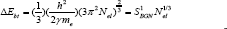
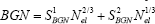
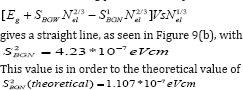
Where ‘ћ’ is the Planck's constant and  is the ratio for of reduced effective mass to free-electron mass, which is equal to 0.274 for pure CdO. Therefore, the value of the coefficient is sbgn = 4.49X10⁻¹⁵eVcm2 . It is seen in Figure 9(a) the s1bon in present case obtained is 3.07 x 10⁻¹⁵ eVcm2 which is close to the theoretical value.
Figure 9: Plot of Eg - Ego Vs n2/3 and optoelectronic function for CdO film.

The second part of BGN results from the Columbic interaction (C-int) between carriers and is given by [29]
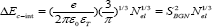
where εo is the permittivity of free space, e is the electronic charge, and εr is the dielectric constant . Thus

Therefore, the total BGN is equal to
The bandgap shift can be determined mainly by the BGN effects, as

Where Cf is a fitting parameter The plot of
The difference might come from the non-parabolic band effects [29] The IR reflectivity is one of the main requirements for a high quality solar window material. The efficiency of flat collector reduces considerably because of the escape of the thermal energy in the form of IR radiation the TCO having high reflectivity can be used to overcome this difficulty the IR reflectivity is calculated using relation [14].

The value of 1/εo co= 376 Ω the free space impedance the reflectivity of the film oscillates over 94 - 96 % and this is along with good transmittance suggest that films are used in window layer in solar cell, in different optoelectronic devices like in flat panel displays, collectors photo thermal conversion and work electrode in electrode position processes. The IR reflectivity obtained by using above relation for 0.025 M - 0.125 M CdO thin films are 65.95 %, 94.79 %, 95.98 %, 97.97 % and 91.82 % .The highest reflectivity of 97.97 % obtained for 0.1 M CdO thin film, make it suitable candidate for applications in heat reflecting mirrors.
The degeneracy of the films confirmed by evaluation of Fermi energy using formula [14]

Where m* is the value of effective mass = 0.21 me in case of CdO. The degeneracy can be confirmed by comparing values of EF with kT if Ef >> kT , it means films are degenerate. Secondly by plotting graph of EF Vs n, if the graph is linear the semiconductor is degenerate. Figure 10 shows the plot of Fermi energy (EF) Vs carrier concentration (n) for CdO film which is straight line it means the CdO has degenerate semiconducting nature.
Figure 10: Typical plot of EF Vs n to determine degeneracy of CdO film material for all the CdO films prepared with different concentration.

The free path in TCO film may interact with different scattering centers like thermal vibration of the lattice, ionized and neutral impurities and the grain boundary regions. For degenerate semiconductor the ionized impurity and grain boundary scattering are important than the scattering by neutral impurity. If there is mismatch between the mean free path and the crystallite size it means that the grain boundary scattering is not dominant mechanism, in that case the other scattering mechanism like lattice scattering, impurity scattering mechanisms are more dominant which affect the electrical conductivity. The mean free path is calculated by using following formula [14].

Where symbols have usual meaning. The calculated values of T are depicted in (Table 2). In case of CdO film deposited with various concentrations of 0.025 M to 0.125 M at 350 oC substrate temperature, the calculated values of mean free length for 0.05 M, 0.075 M and 0.125 M CdO film are nearly matches with the crystallite size given in (Table 1), therefore, it is concluded that the grain boundary scattering is dominant phenomenon for obtained mobility values whereas in 0.025 M and 0.1 M CdO films the lattice scattering, impurity scattering are dominant phenomenon.
Another important scattering mechanism responsible for electrical properties is ionized impurity scattering which can be checked by calculating and comparing the mobility values experimentally obtained with the mobilities of ionized impurity [14].

It is observed that there is much difference in the experimentally obtained mobility values of CdO film and calculated mobility values using above relation, therefore, it is concluded that the ionized impurity scattering is not dominant phenomenon in present case. The values of experimental and calculated mobilities are depicted in (Table 2).
The variation of electrical resistivity (ρ), carrier concentration (n) and mobility (μ) of 0.025 M to 0.125 M CdO thin films measured at room temperature by four point probe Hall method in standard van der Pauw configuration is presented in (Table 2). The resistivity decreases from 34.5 x 10⁻⁴ to 1.25 x 10⁻⁴ Ωcm with increase in precursor concentration for 0.025 M to 0.125 M CdO film. The decrement in the electrical resistivity of the CdO thin films with the increase in concentration of precursor concentration is due to increment in crystallinity, enhancement in carrier concentration and mobility of charge carriers. It is well known that the nature of defects and grain boundaries of different thin films are strongly dependent on the crystal quality.
The defects and grain boundary acts as free electron trap centers, which reduces the charge carrier concentration and become scattering centers, leading to a decrease in electrical mobility. These reported values of resistivity are very small compared to the results obtained for CdO thin films obtained by various physical and chemical methods [28-30]. (Figure 11) shows the variation of carrier concentration and mobility for 0.025 M to 0.125 M CdO thin films deposited at 350oC substrate temperature.
Figure 11: The variation of carrier concentration and mobility of CdO films deposited at 350 oC for 0.025 M - 0.125 M precursor concentrations.

From the point of view of application of transparent conducting oxide in optoelectronic devices, figure of merit (Ф) is one of the important parameter, which is calculated from well known Haackes formula [31]. The figure of merit (Ф) for 0.1 M CdO is the highest compared to the reported value of Ф for CdO thin films prepared by various chemical and physical thin film deposition technique, in this study it is 25.3 x 10⁻³ (Ω)-1. It is observed that figure of merit increases with increase in concentration up to 0.1 M CdO thin film and then decreases due to increase in sheet resistance and increase in crystallite size as shown in (Figure 12). The sheet resistance (Rs), thickness (t), transmittance (T), figure of merit (Ф), resistivity (ρ), carrier concentration (n), mobility (μ), Fermi energy (EF), IR reflectivity (R), and free path length (l) are presented in (Table 2).
Figure 12: The variation of figure of merit ® and R s of 0.025M - 0.125M CdO thin films deposited at 350 oC substrate temperature.

(Figure 13) shows the room temperature PL spectra of CdO thin films deposited with different precursor concentration. Two emission peaks at 434 nm and 539.80 nm (green) are observed significantly for 0.075 M and 0.1 M CdO thin films when films are excited at 400 nm wavelength which is due to the combination of electron and hole from the conduction and valance band whereas for 0.025 M and 0.05 M CdO film the peaks are observed at 429.34 and 535.44 nm wavelength of which intensity is less due their high band gap energy. The peak at 539.8 nm arises due to the oxygen vacancies in CdO thin films; because photo generated holes in valence band recombine with an electron in conduction band [32].
Figure 13: PL spectra of CdO films of 0.025 M-0.125 M precursor concentrations deposited at 350 oC substrate temperature.

CdO thin films have been deposited on glass substrate with different concentration of cadmium precursor solution by SPT. It is noteworthy that the concentration of precursor solution plays an important role in changing the properties of CdO thin films. The XRD study reveal that all the CdO films are polycrystalline face centered cubic in nature, textured along (111) and (200) planes, minimum value of strain 1.95 x 10⁻³ and dislocation density 0.785 x 10¹⁵ lines /m2 confirms high degree of crystallization present for 0. 1.M CdO film. Surface morphology of films changed from rough to smooth and thickness of the films increases from 794 nm to 1523 nm, as cadmium content increased with concentration of spraying solution. Presence of Cd in Cd+1 state confirms oxygen deficiency which is responsible for the better electrical conductivity of CdO thin films. The optical direct band gap decreases from 2.58 eV to 2.42 eV with increase in precursor concentration is due to BGN related to M-B shift. The highest reflectivity of 97.97 % obtained for 0.1 M CdO thin film, make it suitable candidate for applications in heat reflecting mirrors. All the CdO films show n-type semiconducting behavior with electrical resistivity lies in the range of 34.5 x 10⁻⁴ to 2.7 x 10⁻⁴ Ωcm. The film deposited of 0.1 M concentration exhibits the highest figure of merit 25.3 x 10⁻³ (Ω)-1, carrier concentration of 5.87 x 10²⁰ /cm3 and mobility of 40 cm/Vs. Two photoemission wavelengths are observed at 434 and 539.80 nm when excited at 400nm wavelength. These improved electrical parameters of films make them useful in optoelectronic applications.
Dr AV Moholkar is grateful to DAE-BRNS, Mumbai, India for financial assistance through Major research project No.2013/36/29- BRNS/2351.